New prod uc t al8808, Recommended operating conditions, Electrical characteristics – Diodes AL8808 User Manual
Page 3
AL8808
Document number: DS35648 Rev. 2 - 2
3 of 20
January 2013
© Diodes Incorporated
NEW PROD
UC
T
AL8808
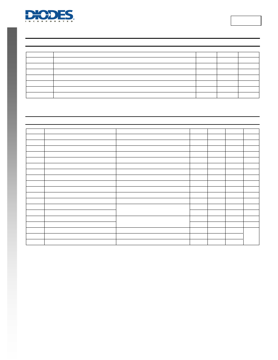
Recommended Operating Conditions
(@T
A
= +25°C, unless otherwise specified.)
Symbol
Parameter
Min
Max
Unit
V
IN
Operating Input Voltage Relative to GND
6.0 30 V
V
CTRLH
Voltage High for PWM Dimming Relative to GND
2.6
5.5
V
V
CTRLDC
Voltage Range for 20% to 100% DC Dimming Relative to GND
0.5
2.5
V
V
CTRLL
Voltage Low for PWM Dimming Relative to GND
0
0.4
V
I
SW
Continuous Switch Current (Note 4)
1
A
f
SW
Maximum Switching Frequency
1
MHz
T
J
Junction Temperature Range
-40
+125
°C
Note:
4. Subject to ambient temperature, input voltage and switching frequency. See applications section for suggested derating.
Electrical Characteristics
(@ T
A
= +25°C, V
IN
= 12V, CTRL pin floating; unless otherwise specified.)
Symbol Parameter
Conditions Min
Typ
Max
Unit
V
INSU
Internal Regulator Start Up Voltage
V
IN
rising
5.6
V
V
INSH
Internal Regulator Hysteresis Threshold
V
IN
falling
200
mV
I
Q
Quiescent Current
V
IN
= 30V, output not switching
350
µA
I
S
Input Supply Current
f
SW
= 250kHz
450
µA
V
TH
Set Current Threshold Voltage
95
100
105
mV
V
TH-H
Set Threshold Hysteresis
±20
mV
I
SET
SET Pin Input Current
V
SET
= V
IN
-0.1
16
µA
V
CTRL
Open Circuit CTRL Pin Voltage
5
V
R
CTRL
CTRL Pin Input Resistance
Referred to internal 5V regulator.
50
kΩ
V
REF
Internal Reference Voltage
2.5
V
R
DS(on)
On Resistance of SW MOSFET
I
SW
= 0.35A
0.35
Ω
I
SW_Lkg
Switch Leakage Current
V
IN
= 30V, V
CTRL
= 0.4V, V
SENSE
= 0V
0.5
µA
t
R
SW Rise Time
V
SENSE
= 100 ±20mV, f
SW
= 250kHz
V
SW
= 0.1V to 12V to 0.1V, C
L
= 15pF
7
ns
t
F
SW Fall Time
5
ns
T
OTP
Over-Temperature Shutdown
145
°C
T
OTP-Hyst
Over-Temperature Hysteresis
10
°C
θ
JA
Thermal Resistance Junction-to-Ambient
TSOT25 (Note 5)
209
°C/W
θ
JL
Thermal Resistance Junction-to-Lead
TSOT25 (Note 5)
57
θ
JT
Thermal Resistance Junction-to-Top
TSOT25 (Note 5)
13
Notes:
5. Device mounted on FR-4 PCB (25mm x 25mm 1oz copper, minimum recommended pad layout on top layer and thermal vias to maximum area
bottom layer ground plane. For better thermal performance, larger copper pad for heat-sink is needed.
…Refer to Figure 42 for the device derating curve.