New prod uc t, Applicatio, On informat – Diodes AL8808 User Manual
Page 16: Tion, Al8808
NEW PROD
UC
T
AL8808
Document number
Applicatio
EMI and Layo
The AL8808 is
decoupling and
switching speed
due to switching
The turn-on edg
and PCB tracks
between the Sch
The tracks from
short as possible
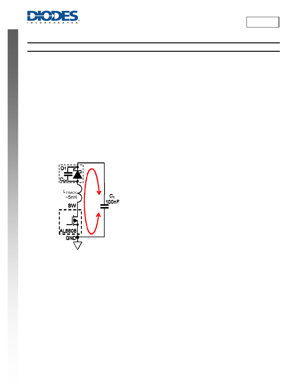
There is an indu
estimate the prim
and length will d
The resonant fre
diode. An exam
Summary:
1. Use
a
the gr
(EMC
2. Place
less th
the in
parasi
more g
3. Place
4. Place
5. Place
capac
imped
r: DS35648 Rev. 2
on Informat
out Considerat
a switching reg
layout of the PC
ds of the internal
g losses and radia
ge (falling edge)
. After the Scho
hottky diode capa
the SW pin to t
e.
uctance internally
mary resonant fr
dominate the size
equency of any
mple of good layo
Figure 43. PC
PCB constructio
round areas are
) operation and a
capacitor C1 as
han about 5mm.
put current pass
itic inductance of
ground via holes
sense resistor R
D1 anode, the S
capacitor C2 as
citor and its copp
dance coupling d
- 2
tion
(cont.)
tions
ulator with fast
CB.To help with
power MOSFET
ated EMI.
dominates the ra
ottky diode revers
acitance and the
the Anode of the
y in the AL8808 t
equency. If the t
e of the inductanc
oscillation is det
ut is shown in Fi
CB Loop Reson
on with copper fo
tightly connecte
also to minimize
close as possib
To ensure the b
ses directly throu
f the copper trac
s close to the gro
R1 as close as po
SW pin and the in
s close as poss
per trace such tha
ue to the added
edges and mea
these effects the
T. The rise and
adiated EMI whi
se recovery time
e track inductanc
e Schottky diode
this can be assu
rack is capable o
ce.
termined by the
gure 44 - the str
ance
oil on top and bo
ed together using
device temperat
le to V
IN
, and as
best possible EM
ugh the capacito
ce. Ensure low in
ound pad.
ossible to V
IN
and
nductor as close
ible to L1 and S
at the input curre
parasitic inducta
16 of 20
asures small diff
e AL8808 has b
d fall times are c
ch is due to an i
of around 5ns h
e, L
TRACK
, See F
e, D1, and then f
med to be aroun
of handling 1A in
combined induc
ay track inductan
ottom. Provide m
g plated via hole
tures by spreadin
close as possib
MI filtering (greate
r mounting pad.
nductance conne
d SET.
together as poss
SET. To ensure
ent passes direc
ance of the coppe
ferential voltages
een developed t
controlled to get
interaction betwe
has occurred; the
Figure 43.
from D1’s cathod
nd 1nH. For PCB
ncreasing the thic
ctance in the tra
nce should be le
Figure
maximum coverag
es placed at reg
ng the dissipated
le to the cathode
est attenuation),
This minimizes
ection between th
sible to avoid rin
e the best possib
ctly through the c
er trace.
s; as a result of
to minimise radia
the right compro
een the Schottky
e falling edge of
de to the decoup
B tracks a figure
ckness will have
ck and the effec
ss than 5nH.
44. Recommen
ge of copper gro
ular intervals. T
d heat.
e of D1. The sep
place the capaci
s common imped
he capacitor and
ging.
ble EMI filtering
capacitor mountin
f this care has
ated emissions b
omise between p
y diode (D1), Sw
the SW pin sees
pling capacitors
of 0.5nH per mm
e a minor effect o
ctive capacitance
nded PCB Layo
und plane on bo
This is required
paration of these
itor and its coppe
dance coupling d
d its ground conn
(greatest attenu
ng pad. This mi
January 201
© Diodes Incorporate
AL8808
to be taken with
by controlling the
power dissipation
witching MOSFET
s a resonant loop
C1 should be as
m can be used to
on the inductance
e of the Schottky
ut
oth sides. Ensure
both for low EM
nodes should be
er trace such tha
due to the added
nection. Use 2 o
uation), place the
nimizes common
3
ed
h
e
n
T
p
s
o
e
y
e
MI
e
at
d
or
e
n