New prod uc t, Pin descri, Functiona – Diodes AL8808 User Manual
Page 2: Absolute m, Iptions, Al block dia maximum, Agram, Ratings, Al8808
NEW PROD
UC
T
AL8808
Document number
Pin Descri
Pin Number
1
2
3
4
5
Functiona
Absolute M
Symbol
ESD HBM
ESD MM
V
IN
V
SET
V
SW
V
CTRL
I
SW
T
J
T
LEAD
T
ST
Caution: Stresse
function
affecte
Semico
and tra
r: DS35648 Rev. 2
iptions
Pin Name
SW
GND
CTRL
SET
V
IN
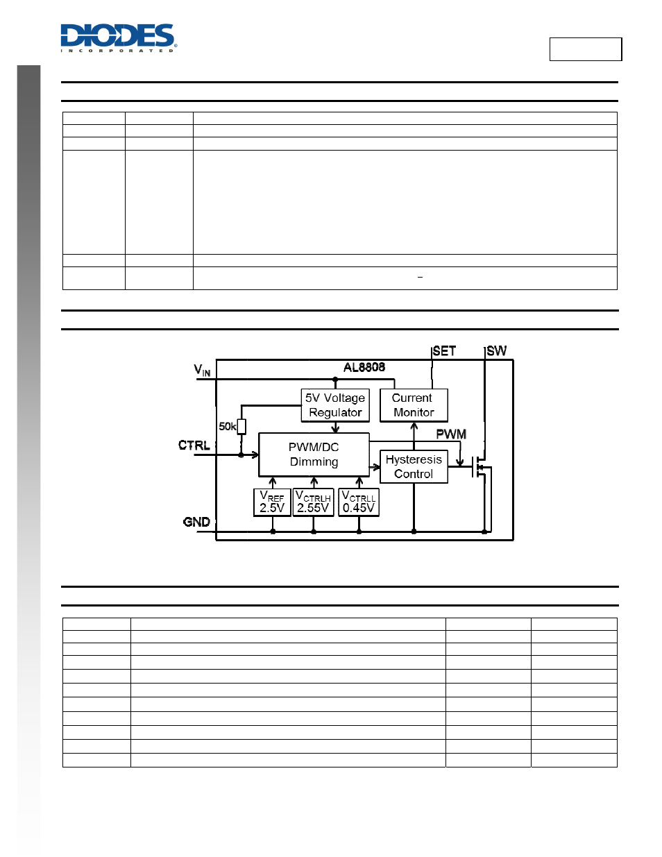
al Block Dia
Maximum
Human Body M
Machine Mode
Continuous V
I
SET pin voltag
SW voltage re
CTRL pin inpu
Switch current
Junction Temp
Lead Tempera
Storage Temp
es greater than the
nal operation of the
d by exposure to a
onductor devices a
ansporting these de
- 2
Switch Pin. C
GND Pin
Dimming and
• Leave
f
(V
• Drive
to
• Drive
w
I
OUTnom
• Drive
w
• A
PWM
current
Set Nominal
Input Supply
section for m
agram
Ratings
(@
Model ESD Prote
el ESD Protectio
N
pin voltage rela
ge relative to V
IN
elative to GND
ut voltage
t
perature
ature Soldering
perature Range
e 'Absolute Maxim
e device at these o
bsolute maximum
are ESD sensitive a
evices.
Connect inductor
d On/Off Control
floating for norma
V
CTRL
= 5V, Give
o voltage below 0
ith an analog vol
m
ith an analog vol
signal (low leve
to be adjusted b
Output Current P
Pin. Must be loc
more information.
Figure 1
T
A
= +25°C, unle
Parameter
ection
n
ative to GND
pin
mum Ratings' spec
or any other condit
rating conditions fo
and may be damag
2 of 20
r/freewheeling dio
Input.
al operation.
es nominal avera
0.4V to turn off ou
ltage (0.5V < V
CT
ltage > 2.6V outp
l ≤ 0.4V and high
below the level se
Pin. Configure th
cally decoupled t
.
AL8808 Block
ess otherwise sp
ified above, may c
tions exceeding tho
or extended periods
ged by exposure to
Function
ode here, minimi
ge output curren
utput current
TRL
< 2.5V) to ad
put current will be
h level > 2.6; tran
et by the resistor
he output current
o GND with > 2.2
k Diagram
pecified.)
cause permanent d
ose indicated in thi
s of time.
o ESD events. Suit
izing track length
nt I
OUTnom
= 0.1/R
djust output curre
e 100% of I
OUTno
nsition times less
r connected to S
of the device.
2µF X7R cerami
Rating
2.5
200
-0.3 to
-5 to +
-0.3 to
-0.3 to
1.25
150
300
-55 to +
damage to the dev
is specification is n
table ESD precaut
h at this pin to red
R
S
)
ent from 20% to
om
s than 1µs) allow
ET input pin.
c capacitor – see
gs
0
+33
0.3
+33
+6
5
0
0
+150
vice. These are st
not implied. Device
ions should be tak
January 201
© Diodes Incorporate
AL8808
duce EMI.
100% of
ws the output
e applications
Unit
kV
V
V
V
V
V
A
°C
°C
°C
tress ratings only;
e reliability may be
ken when handling
3
ed