Electrical characteristics, Al8807a – Diodes AL8807A User Manual
Page 4
AL8807A
Document number: DS35990 Rev. 2 - 2
4 of 20
March 2013
© Diodes Incorporated
AL8807A
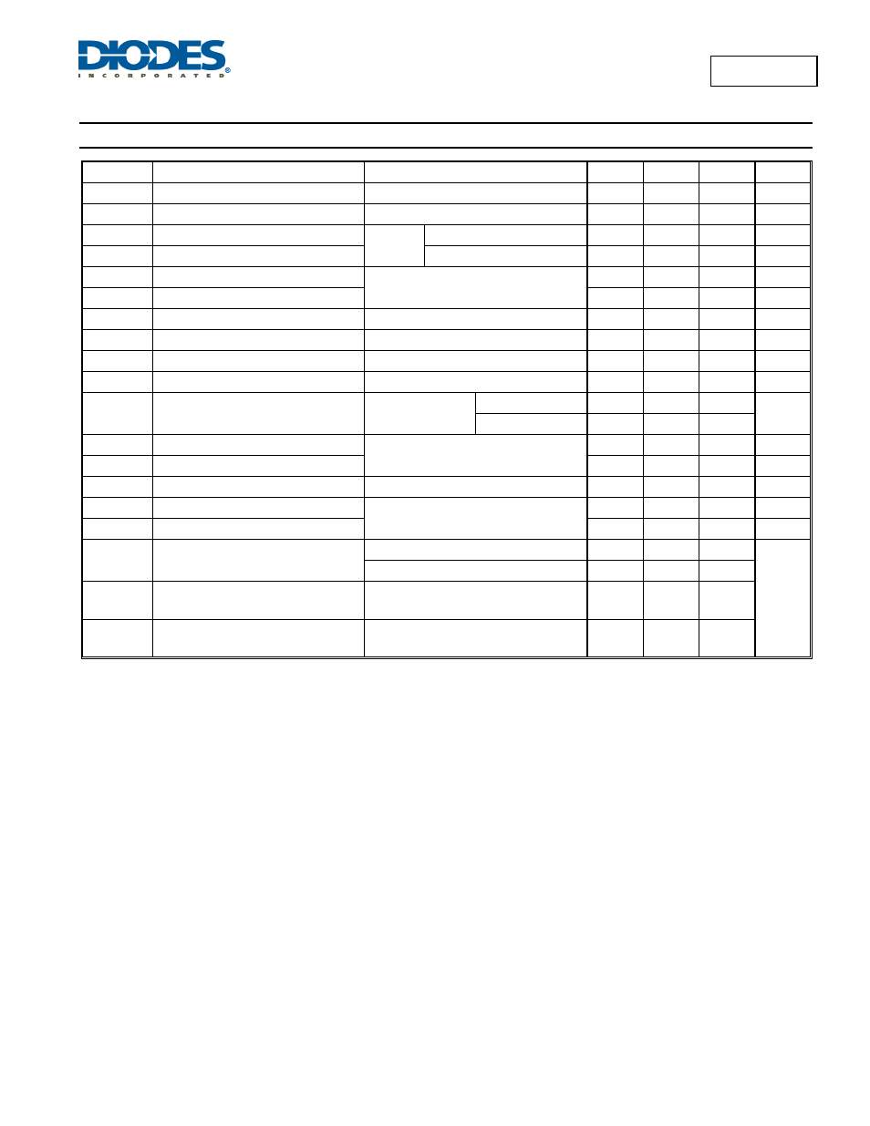
Electrical Characteristics
(@T
A
= +25°C, unless otherwise specified.)
Symbol Parameter
Conditions Min
Typ
Max
Unit
V
INSU
Internal Regulator Start Up Threshold
V
IN
rising
5.9
V
V
INSH
Internal Regulator Hysteresis Threshold V
IN
falling
100 300
mV
I
Q
Quiescent Current
CTRL pin
floating
Output not switching (Note 6)
350
µA
I
S
Input Supply Current
f = 250kHz
1.8
5
mA
V
TH
Set Current Threshold Voltage
CTRL pin floating
95 100 105 mV
V
TH-H
Set Threshold Hysteresis
±20
%
V
TH-10%
10% Set Current Threshold Voltage
V
CTRL
= 0.25V
4 10 15
mV
I
SET
SET Pin Input Current
V
SET
= V
IN
-0.1
16
22
µA
R
CTRL
CTRL Pin Input Resistance
Referred to internal reference
50
k
Ω
V
REF
Internal Reference Voltage
2.5
V
R
DS(on)
On Resistance of SW MOSFET
I
SW
= 0.3A
SOT25
0.25
0.40
Ω
MSOP-8EP
0.18
0.35
t
R
SW Rise Time
V
SENSE
= 100 ±20mV, f
SW
= 250kHz
V
SW
= 0.1V ~ 12V ~ 0.1V, C
L
= 15pF
12 ns
t
F
SW Fall Time
20 ns
I
SW_Leakage
Switch Leakage Current
V
IN
= 36V
0.5
μA
T
OTP
Over-Temperature Shutdown
150
C
T
OTP-Hyst
Over-Temperature Hysteresis
25
C
JA
Thermal Resistance Junction-to-Ambient
(Note 7)
SOT25 (Note 8)
250
°C/W
MSOP-8EP (Note 9)
69
JL
Thermal Resistance Junction-to-Lead
(Note 10)
SOT25 (Note 8)
50
JC
Thermal Resistance Junction-to-case
(Note 11)
MSOP-8EP (Note 9)
4.3
Notes:
6. AL8807A does not have a low power standby mode but current consumption is reduced when output is not being switched.
7. Refer to Figure 40 for the device derating curve.
8. Test condition for SOT25: Device mounted on FR-4 PCB (25mm x 25mm 1oz copper, minimum recommended pad layout on top layer and thermal
vias to bottom layer ground plane. For better thermal performance, larger copper pad for heat-sink is needed.
9. Test condition for MSOP-8EP: Device mounted on FR-4 PCB (51mm x 51mm 2oz copper, minimum recommended pad layout on top layer and
thermal vias to bottom layer with maximum area ground plane. For better thermal performance, larger copper pad for heat-sink is needed.
10. Dominant conduction path via Gnd pin (pin 2).
11. Dominant conduction path via exposed pad.