Al8807a, Application information, On off – Diodes AL8807A User Manual
Page 14
AL8807A
Document number: DS35990 Rev. 2 - 2
14 of 20
March 2013
© Diodes Incorporated
AL8807A
Application Information
(cont.)
The inductor value should be chosen to maintain operating duty cycle and switch 'on'/'off' times over the supply voltage and load current range.
The following equations can be used as a guide, with reference to Figure 39 – typical switching waveform.
Switch ‘On’ time
R
r
R
x
I
V
V
I
L
t
SW
L
S
AVG
LED
IN
ON
Switch ‘Off’ time
r
R
x
I
V
V
I
L
t
L
S
AVG
D
LED
OFF
Where:
L is the coil inductance (H)
r
L
is the coil resistance (
Ω)
R
S
is the current sense resistance (
Ω)
I
avg
is the required LED current (A)
ΔI is the coil peak-peak ripple current (A)
{Internally set to 0.3 x Iavg}
V
IN
is the supply voltage (V)
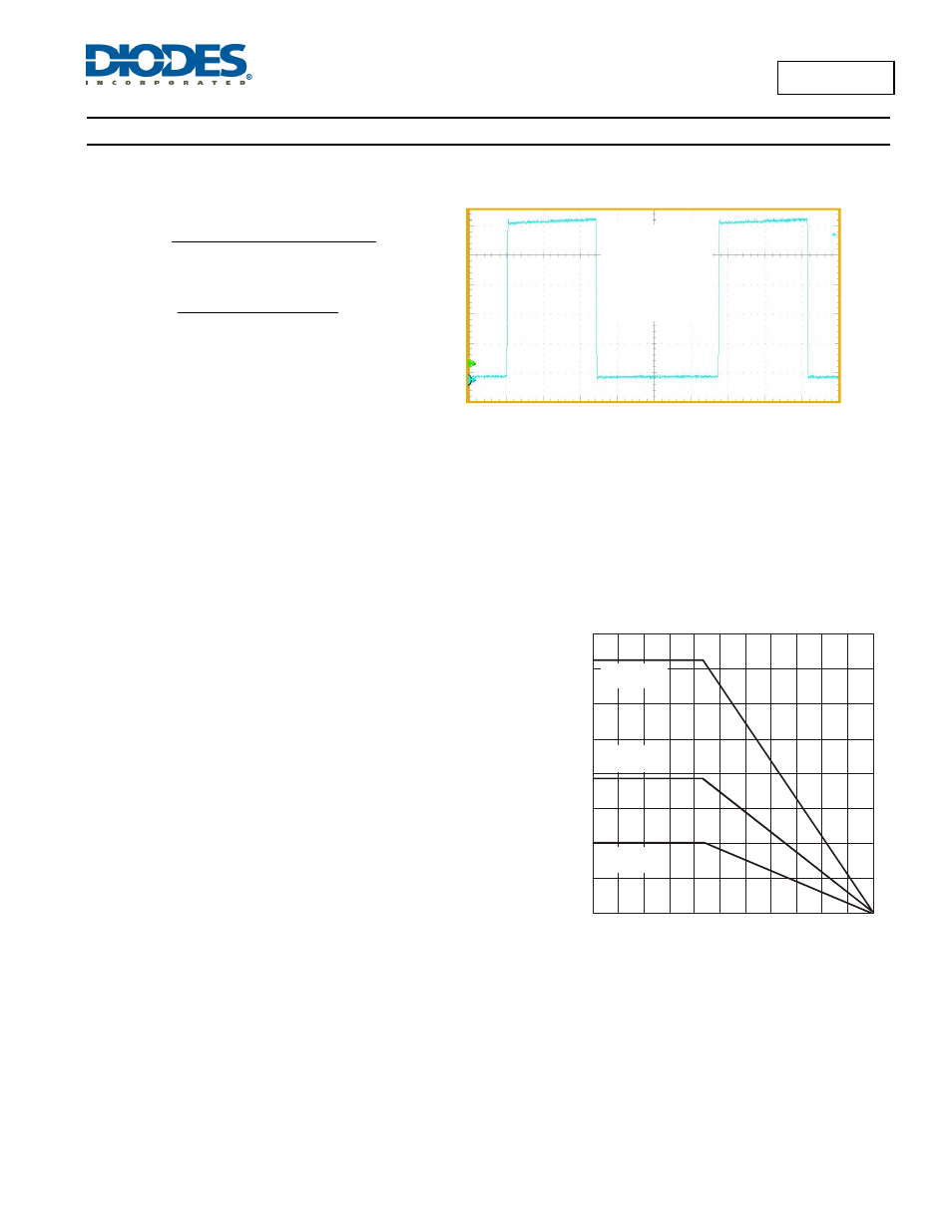
Figure 39 Typical Switching Waveform
V
LED
is the total LED forward voltage (V)
R
SW
is the switch resistance (
Ω) {= 0.25Ω nominal (SOT25)}
V
D
is the diode forward voltage at the required load current (V)
Thermal Considerations
For continuous conduction mode of operation, the absolute maximum junction temperature must not be exceeded. The maximum power
dissipation depends on several factors: the thermal resistance of the IC package
JA
, PCB layout, airflow surrounding the IC, and difference
between junction and ambient temperature.
The maximum power dissipation can be calculated using the following
formula:
P
D(MAX)
= (T
J(MAX)
− T
A
) /
JA
where
T
J(MAX)
is the maximum operating junction temperature,
T
A
is the ambient temperature,
JA
is the junction to ambient thermal resistance.
The recommended maximum operating junction temperature, T
J
, is +125°C
and so maximum ambient temperature is determined by the AL8807A’s
junction to ambient thermal resistance,
JA
and device power dissipation.
JA
, is layout dependent and package dependent; the AL8807AW5’s
JA
on a
25 x 25mm single layer PCB with 1oz copper standing in still air is
approximately +250°C/W and around 130°C/W on a 51mm x 51mm dual layer
board with maximum coverage top and bottom and 3 vias.
The maximum power dissipation at T
A
= +25°C can be calculated by the
following formulas:
P
D(MAX)
= (+125°C
− +25°C) / (250°C/W) = 0.4W for single-layer 25mm x25mm PCB
P
D(MAX)
= (+125°C
− +25°C) / (130°C/W) =0.77W for dual layer 51mm x 51mm PCB
Figure 40, shows the power derating of the AL8807AW5 on two different PCBs and the AL8807AMP on one PCB.
SOT25 – 25mm x 25mm: AL8807AW5’s
JA
on a 25 x 25mm single layer PCB with 1oz copper
SOT25 – 25mm x 25mm: AL8807AW5’s
JA
on a 51mm x 51mm dual layer board with maximum coverage top and bottom and 3 vias
MSOP-8EP - 51mm x 51mm: AL8807AMP’s
JA
on a 51mm x 51mm dual layer board with maximum coverage top and bottom and 4 vias
Figure 40 shows that the MSOP-8EP version of the AL8807A can handle more power than its SOT25 version. So the AL8807AMP is the
preferred variant when operating at larger supply voltage rails (>24V) and/or driving larger LED currents. This is especially true in high power
density/space constraint applications such as high power 24VAC MR16 applications.
V
IN
= 12V
T
A
=25ºC
2 LEDs
20ns/div
SW Pin: 2V/div
On
Off
0
0.2
0.4
0.6
0.8
1.2
1.4
1.6
-40 -25 -10
5
20
35
50
65
80
95 110 125
1.0
MSOP-8EP
51mm x 51mm
SOT25
51mm x 51mm
SOT25
25mm x 25mm
P
O
WE
R
DIS
S
IP
A
T
IO
N (
W
)
AMBIENT TEMPERATURE (°C)
Figure 40 Derating Curve for Different PCB