Al8807a, Absolute maximum ratings, Recommended operating conditions – Diodes AL8807A User Manual
Page 3
AL8807A
Document number: DS35990 Rev. 2 - 2
3 of 20
March 2013
© Diodes Incorporated
AL8807A
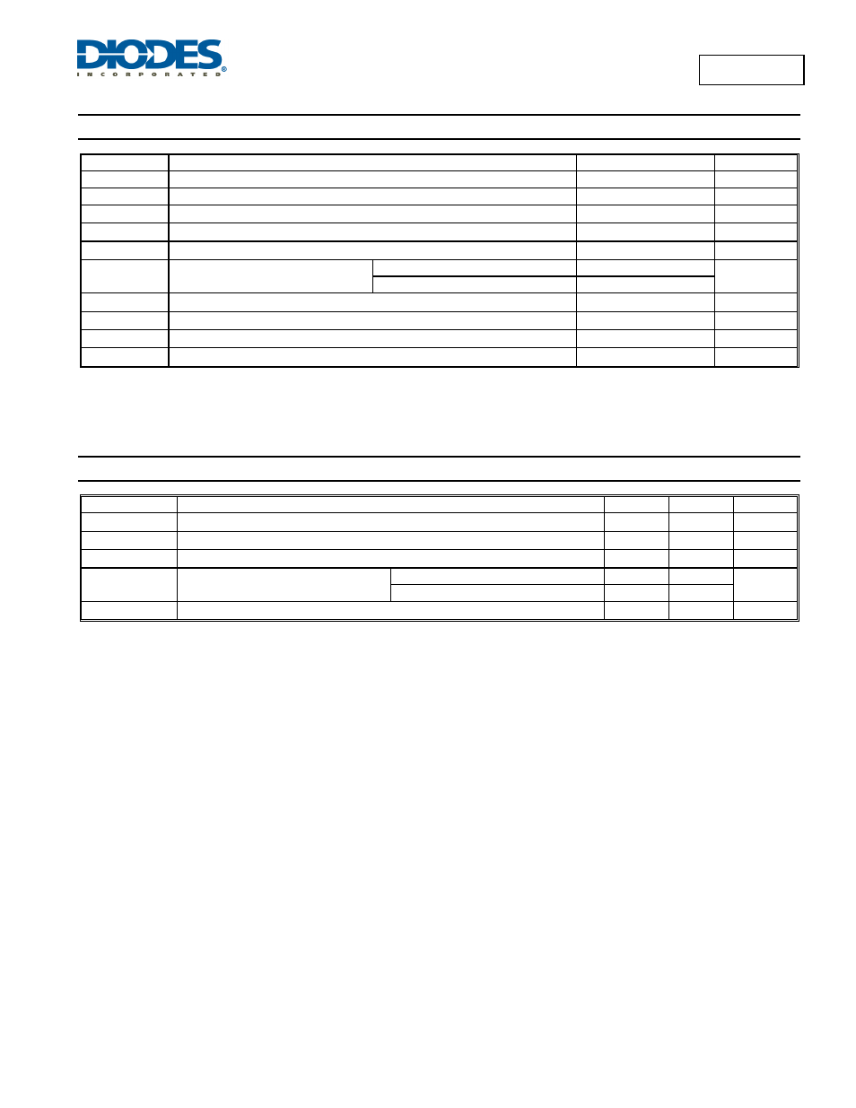
Absolute Maximum Ratings
(@T
A
= +25°C, unless otherwise specified.)
Symbol Parameter
Ratings
Unit
ESD HBM
Human Body Model ESD Protection
2.5
kV
ESD MM
Machine Model ESD Protection
200
V
V
IN
Continuous V
IN
Pin Voltage Relative to GND
-0.3 to +40
V
V
SW
SW Voltage Relative to GND
-0.3 to +40
V
V
CTRL
CTRL Pin Input Voltage
-0.3 to +6.0
V
I
SW-RMS
DC or RMS Switch Current
SOT25 1.25
A
MSOP-8EP 1.5
I
SW-PK
Peak Switch Current (< 10% duty cycle)
2.5
A
T
J
Junction Temperature
150
°C
T
LEAD
Lead Temperature Soldering
300
°C
T
ST
Storage Temperature Range
-65 to +150
°C
Caution:
Stresses greater than the 'Absolute Maximum Ratings' specified above, may cause permanent damage to the device. These are stress ratings only;
functional operation of the device at these or any other conditions exceeding those indicated in this specification is not implied. Device reliability may be
affected by exposure to absolute maximum rating conditions for extended periods of time.
Semiconductor devices are ESD sensitive and may be damaged by exposure to ESD events. Suitable ESD precautions should be taken when handling
and transporting these devices.
Recommended Operating Conditions
(@T
A
= +25°C, unless otherwise specified.)
Symbol
Parameter
Min
Max
Unit
V
IN
Operating Input Voltage
6.0
36
V
V
CTRL
CTRL Pin Input Voltage Range for 10% to 100% ANALOG Dimming (Note 4)
0.25
2.50
V
f
SW
Maximum Switching Frequency at 100% dimming
0.7
MHz
I
SW
Continuous Switch Current (Note 5)
SOT25
1
A
MSOP-8EP
1.3
T
J
Junction Temperature Range
-40
+125
°C
Notes:
4. AL8807A analog dimming range extends below 10% but at reduced LED current accuracies and may not turn completely off. Switching frequencies will
also be increased.
5. Maximum switch current is dependent on power dissipation and junction temperature.