Ap3154a, Pin descriptions, Block diagram – Diodes AP3154A User Manual
Page 3: 120ma high efficiency white led driver
AP3154A
120mA HIGH EFFICIENCY WHITE LED DRIVER
AP3154A Rev. 1
3
of
14
AUGUST 2009
©
Diodes Incorporated
Pin Descriptions
Pin Name
Pin #
Description
D4
1
Current Sink Input #4. Connect to V
OUT
when un-used.
SDI
2
1-wire Serial Digital Interface Input / PWM input
C1
P
3
Positive Terminal of Flying Capacitor. Connect a 1µF capacitor between C1
P
and C1
N
.
C1
N
4
Negative Terminal of Flying Capacitor.
V
OUT
5
The charge pump output voltage to drive load circuit. Connect a 1µF capacitor
between this pin and ground.
C2
P
6
Positive Terminal of Flying Capacitor. Connect a 1µF capacitor between C2
P
and C2
N
.
C2
N
7
Negative Terminal of Flying Capacitor.
V
IN
8
Input Power Source. Connect a 1µF capacitor between this pin and ground.
GND
9
Ground.
D1
10
Current Sink Input #1. Connect to V
OUT
when un-used.
D2
11
Current Sink Input #2. Connect to V
OUT
when un-used.
D3
12
Current Sink Input #3. Connect to V
OUT
when un-used.
GND
EP PAD
Exposed Pad (bottom). Connect to ground underneath the package.
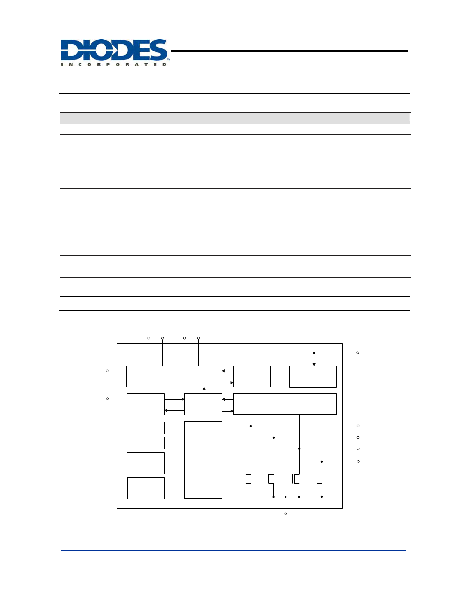
Block Diagram
SHORT
CIRCUIT
PROTECTION
C1
N
C1
P
C2
N
C2
P
V
IN
GND
CURRENT
CONTROL
CHARGE PUMP
SWITCHES
V
OUT
OVER
VOLTAGE
PROTECTION
DIGITAL
CONTROL
BLOCK
SERIAL
DIGITAL
INTERFACE
OUTPUT VOLTAGE REGULATION
&
LED SHORT CIRCUIT DETECTION
SDI
UNDER
VOLTAGE
LOCKOUT
BANDGAP
OSCILLATOR
OVER
TEMPERATURE
PROTECTION
D1
D2
D3
D4