Application information, Hi i – Diodes AL8400 /AL8400Q User Manual
Page 6

AL8400/ AL8400Q
Document number: DS35115 Rev. 4 - 2
6 of 13
August 2012
© Diodes Incorporated
AL8400 /AL8400Q
Application Information
(cont.)
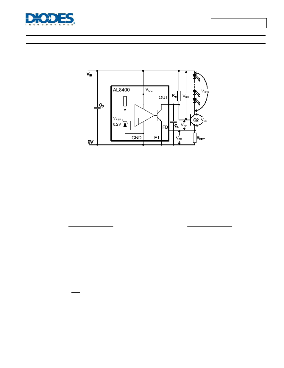
Bipolar Transistor as the Pass Element
For driving currents in the region of about 50mA to about 400mA, the recommended NPN is DNLS320E in the SOT223 package. The high DC
current gain of the DNLS320E is useful in this application, in order to minimize the current in R
B
. The design procedure is as follows, referring to
Figure 4.
Figure 4 Application Circuit Using Bipolar Transistor
There are two important equations for the circuit:
LED Circuit Path:
1. V
CC
= (V
LED
+ V
CE
+ V
FB
) where V
FB
is approximately the internal reference voltage of 200mV.
The maximum total LED voltage plus the reference voltage determines the minimum supply voltage. Substituting into equation 1 yields:
FB
CEsat
max
LED
min
CC
V
V
V
V
+
+
=
where V
LEDmax
is the maximum LED chain voltage.
Control Drive Circuit Path
2. V
CC
= (V
RB
+ V
BE
+ V
FB
)
For a bipolar transistor the voltage (V
RB
) across bias resistor R
B
consists of the base current of Q2 and the output current of the AL8400. So
rearranging equation 2 yields the boundaries for allowable R
B
values:
3.
max
B
min
OUT
FB
max
BE
min
CC
max
B
I
I
V
V
V
R
+
−
−
=
where I
Bmax
is the maximum transistor base current
min
FE
LED
max
B
h
I
I
=
where h
FEmin
is the minimum DC current gain of the transistor.
4.
min
B
max
OUT
FB
min
BE
max
CC
min
B
I
I
V
V
V
R
+
−
−
=
where I
Bmin
is the minimum transistor base current
max
FE
LED
min
B
h
I
I
=
where h
FEmax
is the maximum DC current gain of the transistor.
The value of R
B
should be set somewhere between R
Bmax
and R
Bmin
with the target of trying to get I
OUT
of the AL8400 close to 1mA for nominal
conditions.
Once R
B
has been determined the value for compensation capacitor, C
L
, should be calculated.
B
L
R
ms
2
C
≈
Finally, the bipolar selection is also influenced by the maximum power dissipation
P
TOT
= I
LED
x (V
CC
– V
LED
– V
REF
) = I
LED
x V
CE
Since this determines the package choice (
θ
JA
) in order to keep the junction temperature below the maximum value allowed.
T
J
= T
A
+ P
TOT
x
θ
JA
where
T
J(MAX)
is the maximum operating junction temperature,
T
A
is the ambient temperature,
θ
JA
is the junction to ambient thermal resistance.
