Application information – Diodes AL8400 /AL8400Q User Manual
Page 10
AL8400/ AL8400Q
Document number: DS35115 Rev. 4 - 2
10 of 13
August 2012
© Diodes Incorporated
AL8400 /AL8400Q
Application Information
(cont.)
MOSFET Example Choosing R
B
and C
L
(cont.)
R
Bmax
The minimum recommended I
OUT
for AL8400 is 0.3mA.
The maximum V
GS
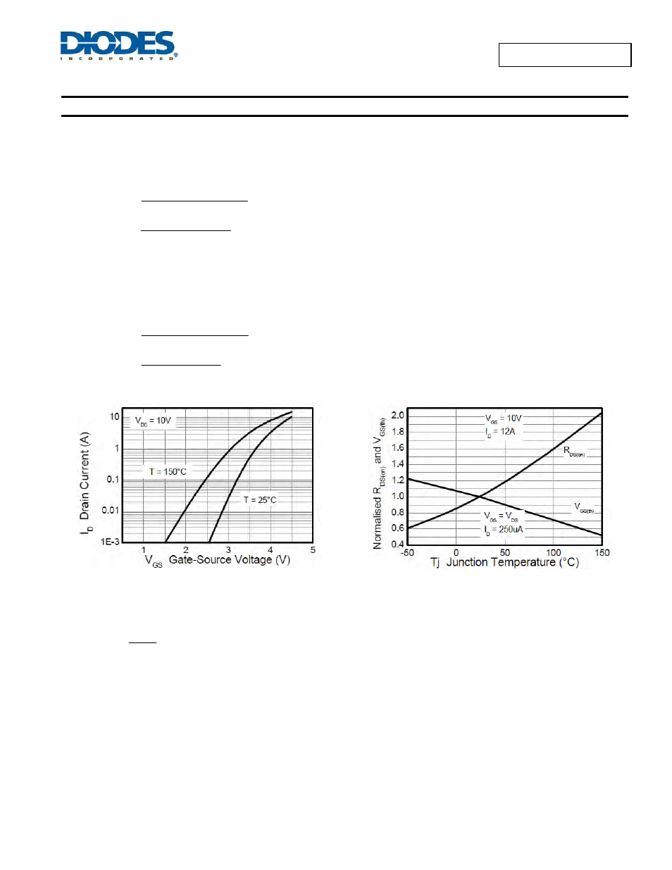
is not stated explicitly, but from the datasheet graphs (Figures 8 and 9) it is expected to be approximately 3.8V at -50°C.
=
−
−
=
min
OUT
FB
max
GS
min
CC
max
B
I
V
V
V
R
=
−
−
=
mA
3
.
0
V
2
.
0
V
8
.
3
V
4
.
11
24.7k
Ω
To ensure that the output capability of the AL8400 is not exceeded at maximum V
IN
and minimum V
GS
these values should be substituted back
into the R
B
equation to determine the minimum allowable value for R
B
.
R
Bmin
The maximum recommended I
OUT
for the AL8400 is 15mA. The minimum V
GS
is about 1V and assuming V
CCmax
= 8.4V:
max
OUT
FB
min
GS
max
CC
min
B
I
V
V
V
R
−
−
=
=
=
mA
15
V
2
.
0
V
1
V
6
.
12
−
−
= 480
Ω
this is less than 12k
Ω and so the AL8400 output current is within its ratings.
Figure 8 Typical Transfer Characteristics
Figure 9 Normalised Curves and Temperature
Assuming V
GS
~ 3V and choosing an R
B
= 8.2k
Ω satisfies the requirements for the AL8400 conformance and sets approximately 1mA in the OUT
pin. The required compensation capacitor can therefore be calculated from:
F
243
.
0
k
2
.
8
ms
2
C
L
μ
≈
Ω
≈
Æ 220nF
The value of R
SET
is V
REF
/I
LED
R
SET
= 0.2/0.2 = 1
Ω
Finally, the maximum power dissipation of the external MOSFET is:
P
TOT
= I
LED
x V
DSMAX
=
I
LED
x (V
CCmax
– V
LEDMIN
– V
FB
)
= 0.2 x( 12.6 – 9 -0.2)
= 0.68W
This determines the package choice (
θ
JA
) in order to keep the junction temperature below the maximum value allowed.
T
J
= T
A
+ P
TOT
x
θ
JA
= 60 + 0.68 x 62.5
= +102.5˚C