New prod uc t ap7175, Electrical characteristics, Ap7175 – Diodes AP7175 User Manual
Page 4
AP7175
Document number: DS35606 Rev. 3 - 2
4 of 14
December 2012
© Diodes Incorporated
NEW PROD
UC
T
AP7175
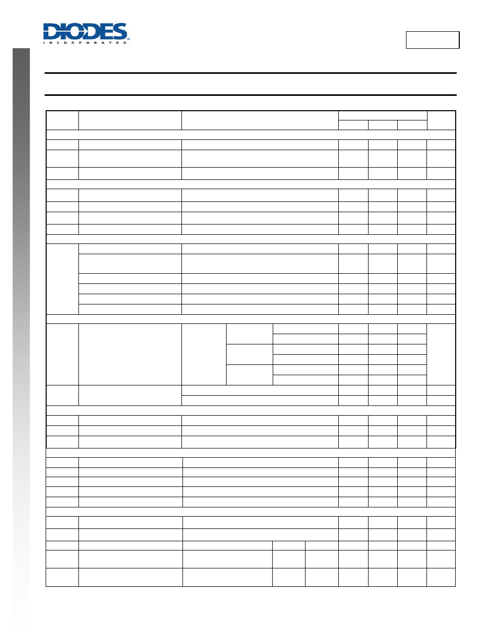
Electrical Characteristics
(V
CNTL
= 5V, V
IN
= 1.8V, V
OUT
= 1.2V and T
A
= -40 to +85°C, @T
A
= +25°C, unless otherwise specified.)
Symbol Parameter
Test
Conditions
AP7175
Unit
Min
Typ
Max
SUPPLY CURRENT
IV
CNTL
V
CNTL
Supply Current
EN = V
CNTL
, I
OUT
=0A
— 1.0 1.5 mA
I
SD
V
CNTL
Supply Current at
Shutdown
EN = GND
—
15
30
µA
V
IN
Supply Current at Shutdown
EN = GND, V
IN
=3.65V
— — 1 µA
POWER-ON-RESET (POR)
Rising V
CNTL
POR Threshold
2.5 2.7 2.95 V
V
CNTL
POR Hysteresis
— 0.4 — V
Rising V
IN
POR Threshold
0.8 0.9 1.0 V
V
IN
POR Hysteresis
— 0.5 — V
OUTPUT VOLTAGE
V
REF
Reference Voltage
FB = V
OUT
— 0.8 — V
Output Voltage Accuracy
V
CNTL
=3.0 ~ 5.5V, I
OUT
= 0 to 3A,
T
J
= -40 to +125°C
-1.5 — +1.5 %
Load Regulation
I
OUT
=0A to 3A
— 0.06
0.25 %
Line Regulation
I
OUT
=10mA, V
CNTL
= 3.0 to 5.5V
-0.15 — +0.15
%/V
V
OUT
Pull-low Resistance
V
CNTL
= 3.3V, V
EN
= 0V, V
OUT
< 0.8V
— 10 —
Ω
FB Input Current
V
FB
= 0.8V
-100 — 100 nA
DROPOUT VOLTAGE
V
DROP
V
IN
-to-V
OUT
Dropout Voltage
(Note 5)
V
CNTL
= 5.0V,
I
OUT
= 3A
V
OUT
= 2.5V
T
J
= +25°C
0.26 0.31
V
T
J
= -40 to +125°C
0.42
V
OUT
= 1.8V
T
J
= +25°C
0.24 0.29
T
J
= -40 to +125°C
0.40
V
OUT
= 1.2V
T
J
= +25°C
0.23 0.28
T
J
= -40 to +125°C
0.38
I
LIM
Current-Limit Level
T
J
= +25°C, V
OUT
= 80% V
NOMiNAL
4.5 5.7 6.7 A
T
J
= -40 to +125°C
4.2 A
PROTECTIONS
I
SHORT
Short Current-Limit Level
V
FB
< 0.2V
— 1.1 — A
T
SD
Thermal Shutdown Temperature
T
J
rising
— 170
°C
Thermal
Shutdown
Hysteresis
— 50 — °C
ENABLE AND SOFT-START
EN Logic High Threshold Voltage
V
EN
rising
0.5 0.8 1.1 V
EN Hysteresis
0.1 — V
EN Pull-High Current
EN = GND
—
5
—
uA
T
SS
Soft-Start Interval
0.3 0.6 1.2 ms
Turn On Delay
From being enabled to V
OUT
rising 10%
200 350 500 us
POWER-GOOD AND DELAY
V
THPG
Rising PG Threshold Voltage
V
FB
rising
90 92 95 %
PG Threshold Hysteresis
—
8
—
%
PG Pull-low Voltage
PG sinks 5mA
—
0.25
0.4
V
PG Debounce Interval
V
FB
< falling PG voltage
threshold
—
10 — µs
PG Delay Time
From V
FB
= V
THPG
to rising
edge of the V
PG
1 2 4 ms
Note:
5. Dropout voltage is the voltage difference between the inut and the output at which the output voltage drops 2% below its nominal value.