New prod uc t ap7175, Pin descriptions, Functional block diagram – Diodes AP7175 User Manual
Page 2
AP7175
Document number: DS35606 Rev. 3 - 2
2 of 14
December 2012
© Diodes Incorporated
NEW PROD
UC
T
AP7175
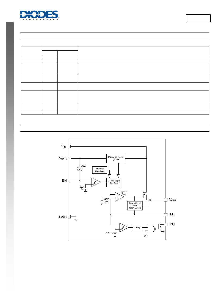
Pin Descriptions
Pin
Name
Pin Number
Function
SO-8EP MSOP-8EP
GND 1 1
Ground
FB 2 2
Feedback to set the output voltage via an external resistor divider between V
OUT
and GND.
V
OUT
3/4 3/4
Power Output Pin. Connect at least 10µF capacitor to this pin to improve transient response and
required for stability. When the part is disabled the output is discharged via an internal pull-low
MOSFET.
V
IN
5 5
Power Input Pin for current supply. Connect a decoupling capacitor (
≥10µF) as close as possible to
the pin for noise filtering.
V
CNTL
6 6
BIAS supply for the controller, recommended 5V. Connect a decoupling capacitor (
≥1µF) as close
as possible to the pin for noise filtering.
PG 7 7
Power Good output open drain to indicate the status of V
OUT
via monitoring the FB pin. This pin is
pulled low when the voltage is outside the limits, during thermal shutdown and if either V
CNTL
or V
IN
go below their thresholds.
EN 8 8
Enable pin. Driving this pin low will disable the part. When left floating an internal current source will
pull this pin high and enable it.
PAD EP EP
Exposed pad connect this to V
IN
for good thermal conductivity.
Functional Block Diagram