New prod uc t ap7175, Absolute maximum ratings, Recommended operating conditions – Diodes AP7175 User Manual
Page 3
AP7175
Document number: DS35606 Rev. 3 - 2
3 of 14
December 2012
© Diodes Incorporated
NEW PROD
UC
T
AP7175
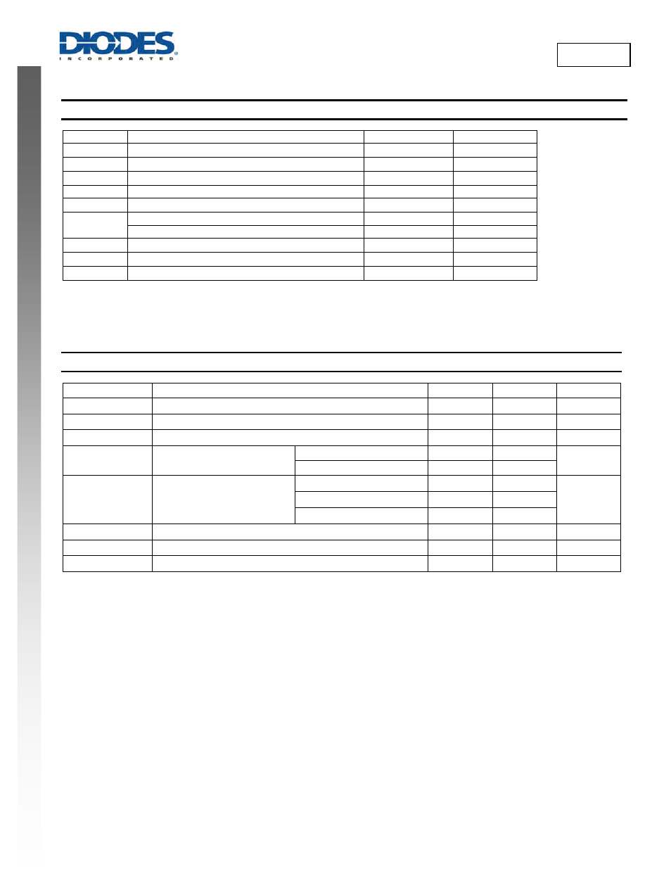
Absolute Maximum Ratings
(Note 4) (@T
A
= +25°C, unless otherwise specified.)
Symbol Parameter
Rating
Unit
V
IN
V
IN
Supply Voltage (V
IN
to GND)
-0.3 to +4.0
V
V
CNTL
V
CNTL
Supply Voltage (V
CNTL
to GND)
-0.3 to +7.0
V
V
OUT
V
OUT
to GND Voltage
-0.3 to V
IN
+0.3
V
PG to GND Voltage
-0.3 to +7.0
V
EN, FB to GND Voltage
-0.3 to V
CNTL
+0.3
V
P
D
Power Dissipation (SO-8EP)
1.7
W
Power Dissipation (MSOP-8EP)
1.5
T
J
Maximum Junction Temperature
150
°C
T
STG
Storage Temperature
-65 to +150
°C
T
SDR
Maximum Lead Soldering Temperature, 10 Seconds
260
°C
Note:
4. Stresses greater than the 'Absolute Maximum Ratings' specified above, may cause permanent damage to the device. These are stress ratings only;
functional operation of the device at these or any other conditions exceeding those indicated in this specification is not implied. Device reliability may
be affected by exposure to absolute maximum rating conditions for extended periods of time.
Recommended Operating Conditions
(@T
A
= +25°C, unless otherwise specified.)
Symbol Parameter Min
Max
Unit
V
CNTL
V
CNTL
Supply Voltage
3.0 5.5 V
V
IN
V
IN
Supply Voltage
1.2 3.65 V
V
OUT
V
OUT
Output Voltage (when V
CNTL
-V
OUT
>1.9V)
0.8
V
IN
- V
DROP
V
I
OUT
V
OUT
Output Current
Continuous Current
0
3
A
Peak Current
0
4
C
OUT
V
OUT
Output Capacitance
I
OUT
= 3A at 25% nominal V
OUT
8 1100
µF
I
OUT
= 2A at 25% nominal V
OUT
8 1700
I
OUT
= 1A at 25% nominal V
OUT
8 2400
E
SRCOUT
ESR of V
OUT
Output Capacitor
0 200
m
Ω
T
A
Ambient Temperature
-40
+85
°C
T
J
Junction Temperature
-40
+125
°C