Electrical characteristics (continued) – Diodes AP2213 User Manual
Page 11
500mA LOW NOISE LDO REGULATOR AP2213
Data Sheet
11
Dec. 2012 Rev. 2. 0
BCD Semiconductor Manufacturing Limited
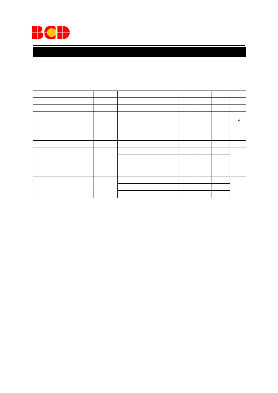
Parameter
Symbol
Conditions
Min
Typ
Max
Unit
Ripple Rejection
PSRR
f=100Hz, I
OUT
=100
μA
75
dB
Current Limit
I
LIMIT
V
OUT
=0V
700
1000
mA
Output Noise
e
no
I
OUT
=50mA, C
OUT
=2.2
μF,
100pF from BYP to GND
260
Enable Input Logic-low
Voltage
V
IL
Regulator shutdown
0.4
V
0.18
Enable Input Logic-high Voltage
V
IH
Regulator enabled
2.0
V
Enable Input Logic-low Current
I
IL
V
IL
≤0.4V
0.01
1
μA
V
IL
≤0.18V
2
Enable Input Logic-high Current
I
IH
V
IL
≥2.0V
5
20
μA
V
IL
≥2.0V
25
Thermal Resistance
θ
JC
TO-252-2 (1)/TO-252-2 (3)
20
o
C/W
SOIC-8
45
SOT-223
31
Hz
nV /
Note 2: Specifications in bold type are limited to -40
o
C
≤T
J
≤125
o
C. Limits over temperature are guaranteed by design, but not
tested in production.
Note 3: Output voltage temperature coefficient is defined as the worst case voltage change divided by the total temperature
range.
Note 4: Regulation is measured at constant junction temperature using low duty cycle pulse testing. Parts are tested for load
regulation in the load range from 0.1mA to 500mA. Changes in output voltage due to heating effects are covered by the thermal
regulation specification.
Note 5: Dropout voltage is defined as the input to output differential at which the output voltage drops 1% (T
J
=25
o
C) or 2% (-
40
o
C
≤T
J
≤125
o
C) below its nominal value measured at 1V differential.
Note 6: Ground pin current is the regulator quiescent current plus pass transistor base current. The total current drawn from the
supply is the sum of the load current plus the ground pin current.
Electrical Characteristics (Continued)
V
IN
=4.3V, I
OUT
=100
μA, C
IN
=1.0
μF, C
OUT
=2.2
μF, V
EN
≥2.0V, T
J
=25
o
C, Bold typeface applies over -40
o
C
≤T
J
≤125
o
C (Note 2),
unless otherwise specified.
AP2213-3.3 Electrical Characteristics