Electrical characteristics – Diodes AP2401/AP2411 User Manual
Page 4
AP2401/AP2411
Document number: DS35113 Rev. 6 - 2
4 of 18
March 2013
© Diodes Incorporated
AP2401/AP2411
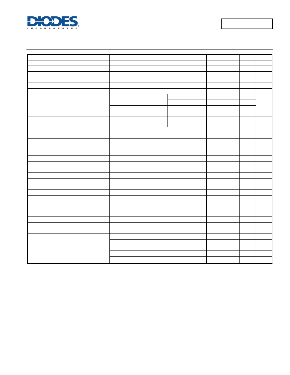
Electrical Characteristics
(@T
A
= +25°C, V
IN
= +5.0V, C
IN
= 0.1µF, C
L
= 1µF, unless otherwise specified.)
Symbol
Parameter
Test Conditions (Note 5)
Min
Typ
Max
Unit
V
UVLO
Input
UVLO
V
IN
rising
1.6
2.0
2.4
V
ΔV
UVLO
Input UVLO Hysteresis
V
IN
decreasing
50
mV
I
SHDN
Input Shutdown Current
Disabled, OUT = open
0.1
1
µA
I
Q
Input Quiescent Current
Enabled, OUT = open
60
100
µA
I
LEAK
Input Leakage Current
Disabled, OUT grounded
0.1
1
µA
I
REV
Reverse Leakage Current
Disabled, V
IN
= 0V, V
OUT
= 5V, I
REV
at V
IN
0.01
1
µA
R
DS(ON)
Switch
on-resistance
V
IN
= 5V, I
OUT
= 2.0A
T
A
= +25°C
70
84
mΩ
-40°C ≤ T
A
≤ +85°C
105
V
IN
= 3.3V, I
OUT
= 2.0A
T
A
= +25°C
90
108
-40°C ≤ T
A
≤ +85°C
135
I
LIMIT
Over-Load Current Limit
(Note 6)
V
IN
= 5V, V
OUT
= 4.5V
-40°C ≤ T
A
≤+85°C 2.05 2.5 2.85 A
I
Trig
Current limiting trigger threshold
Output Current Slew rate (< 100A/s)
2.5
A
I
SHORT
Short-Circuit Current Limit
Enabled into short circuit
2.1
2.75
3.3
A
T
SHORT
Short-circuit Response Time
V
OUT
= 0V to I
OUT
= I
LIMIT
(OUT shorted to ground)
2
µs
V
IL
EN Input Logic Low Voltage
V
IN
= 2.7V to 5.5V
0.8
V
V
IH
EN Input Logic High Voltage
V
IN
= 2.7V to 5.5V
2
V
I
LEAK-EN
EN Input leakage
V
IN
= 5V, V
EN
= 0V and 5.5V
0.01
1
µA
I
LEAK-O
Output leakage current
Disabled, V
OUT
= 0V
0.5
1
µA
T
D(ON)
Output turn-on delay time
C
L
= 1µF, R
LOAD
= 5Ω
0.1 ms
T
R
Output turn-on rise time
C
L
= 1µF, R
LOAD
= 5Ω
0.6
1.5
ms
T
D(OFF)
Output turn-off delay time
C
L
= 1µF, R
LOAD
= 5Ω
0.1 ms
T
F
Output turn-off fall time
C
L
= 1µF, R
LOAD
= 5Ω
0.05
0.1
ms
R
FLG
FLG output FET on-resistance
I
FLG
= 10mA
20
40
Ω
I
FOH
FLG
Off
Current
V
FLG
= 5V
0.01
1
µA
T
BLANK
FLG blanking and latch off time
Assertion or deassertion due to overcurrent and over-
temperature condition
4 7 15
ms
T
DIS
Discharge
time
C
L
= 1µF, V
IN
= 5V, disabled to V
OUT
< 0.5V
0.6
ms
R
DIS
Discharge resistance (Note 7)
V
IN
= 5V, disabled, I
OUT
= 1mA
100
Ω
T
SHDN
Thermal Shutdown Threshold
Enabled
140
°C
T
HYS
Thermal Shutdown Hysteresis
20
°C
θ
JA
Thermal Resistance Junction-to-
Ambient
SO-8 (Note 8)
96
°C/W
MSOP-8 (Note 8)
130
°C/W
MSOP-8EP (Note 9)
92
°C/W
U-DFN3030-8 (Note 9)
84
°C/W
U-DFN2020-6 (Note 10)
90
°C/W
Notes:
6. Pulse-testing techniques maintain junction temperature close to ambient temperature; thermal effects must be taken into account separately.
7. The discharge function is active when the device is disabled (when enable is de-asserted or during power-up power-down when V
IN
< V
UVLO
.
The discharge function offers a resistive discharge path for the external storage capacitor for limited time.
8. Device mounted on 2” x 2” FR-4 substrate PCB, 2oz copper, with minimum recommended pad layout.
9. Device mounted on 2” x 2” FR-4 substrate PCB, 2oz copper, with minimum recommended pad on top layer and thermal vias to bottom layer ground
plane.
10. Device mounted on 1"x1" FR-4 substrate PCB, 2oz copper, with minimum recommended padon top layer and thermal vias to bottom layer ground.