Functional block diagram, Absolute maximum ratings, Recommended operating conditions – Diodes AP2401/AP2411 User Manual
Page 3
AP2401/AP2411
Document number: DS35113 Rev. 6 - 2
3 of 18
March 2013
© Diodes Incorporated
AP2401/AP2411
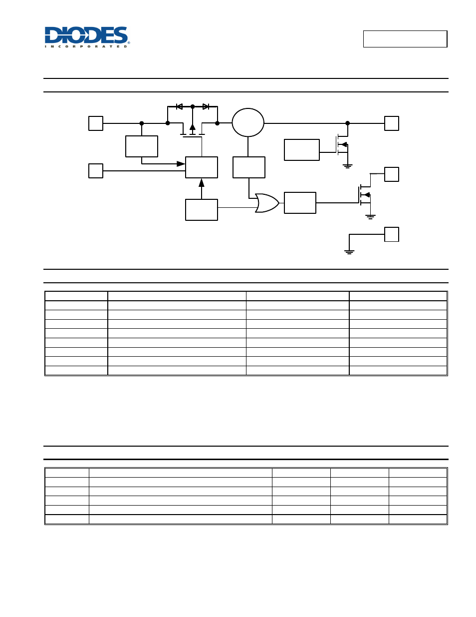
Functional Block Diagram
Thermal
Sense
FLG
OUT
GND
IN
EN
UVLO
Current
Limit
Current
Sense
Deglitch
Discharge
Control
Driver
Absolute Maximum Ratings
(@T
A
= +25°C, unless otherwise specified.)
Symbol Parameter
Ratings
Unit
ESD HBM
Human Body Model ESD Protection
4
kV
ESD MM
Machine Model ESD Protection
300
V
V
IN
Input Voltage (Note 4)
-0.3 to 6.5
V
V
OUT
Output Voltage (Note 4)
-0.3 to V
IN
+0.3 or 6.5
V
V
EN ,
V
FLG
Enable Voltage (Note 4)
-0.3 to V
IN
+0.3 or 6.5
V
I
LOAD
Maximum Continuous Load Current
Internal Limited
A
T
J(MAX)
Maximum Junction Temperature
150
°C
T
ST
Storage Temperature Range (Note 4)
-65 to +150
°C
Notes:
4. All voltages referred to GND pin. Maximums are the lower of V
IN
+ 0.3 and 6.5V
5. UL Recognized Rating from -30°C to +70°C (Diodes qualified T
ST
from -65°C to +150°C).
Caution: Stresses greater than the 'Absolute Maximum Ratings' specified above, may cause permanent damage to the device. These are stress ratings
only; functional operation of the device at these or any other conditions exceeding those indicated in this specification is not implied. Device reliability may
be affected by exposure to absolute maximum rating conditions for extended periods of time.
Semiconductor devices are ESD sensitive and may be damaged by exposure to ESD events. Suitable ESD precautions should be taken when handling
and transporting these devices
Recommended Operating Conditions
(@T
A
= +25°C, unless otherwise specified.)
Symbol Parameter
Min
Max
Unit
V
IN
Input voltage
2.7
5.5
V
I
OUT
Output Current
0
2
A
V
IL
EN Input Logic Low Voltage
0
0.8
V
V
IH
EN Input Logic High Voltage
2
V
IN
V
T
A
Operating Ambient Temperature
-40
+85
°C