Electrical characteristics – Diodes AP2141/ AP2151 User Manual
Page 4
AP2141/ AP2151
Document number: DS31562 Rev. 7 - 2
4 of 17
March 2013
© Diodes Incorporated
AP2141/ AP2151
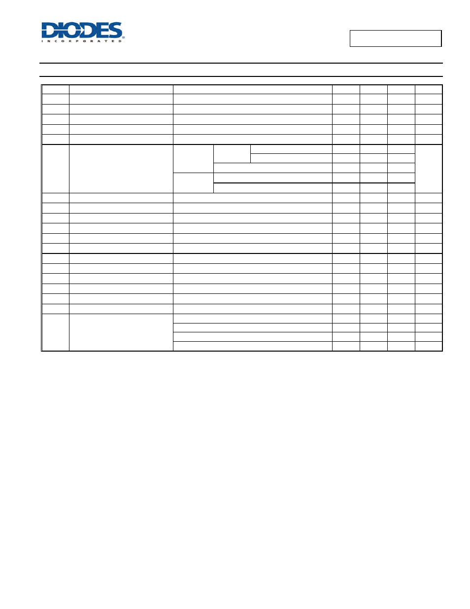
Electrical Characteristics
(@T
A
= +25°C, V
IN
= +5.0V, unless otherwise specified.)
Symbol Parameter
Conditions
Min
Typ
Max
Unit
V
UVLO
Input UVLO
R
LOAD
= 1k
Ω
1.6 1.9 2.5 V
I
SHDN
Input Shutdown Current
Disabled, I
OUT
= 0
0.5 1 µA
I
Q
Input Quiescent Current
Enabled, I
OUT
= 0
45
70
µA
I
LEAK
Input Leakage Current
Disabled, OUT grounded
1
µA
I
REV
Reverse Leakage Current
Disabled, V
IN
= 0V, V
OUT
= 5V, I
REV
at V
IN
1 µA
R
DS(ON)
Switch On-Resistance
V
IN
= 5V,
I
OUT
= 0.5A
T
A
= +25°C
SOT25, SO-8, MSOP-8EP
95
115
m
Ω
U-DFN2018-6
90
110
-40°C
≤ T
A
≤ +85°C
140
V
IN
= 3.3V,
I
OUT
= 0.5A
T
A
= +25°C
120
140
-40°C
≤ T
A
≤ +85°C
170
I
SHORT
Short-Circuit Current Limit
Enabled into short circuit, C
L
= 22µF
0.6 A
I
LIMIT
Over-Load Current Limit
V
IN
= 5V, V
OUT
= 4.8V, C
L
= 22µF, -40
C ≤ T
A
≤ +85°C
0.6 0.8 1.0 A
I
TRIG
Current Limiting Trigger Threshold
Output Current Slew rate (<100A/s) , C
L
= 22µF
1.0 A
I
SINK
EN Input Leakage
V
EN
= 5V
1
µA
t
D(ON)
Output Turn-On Delay Time
C
L
= 1µF, R
LOAD
= 10
Ω
0.05 ms
t
R
Output Turn-On Rise Time
C
L
= 1µF, R
LOAD
= 10
Ω
0.6
1.5
ms
t
D(OFF)
Output Turn-Off delay Time
C
L
= 1µF, R
LOAD
= 10
Ω
0.01 ms
t
F
Output Turn-Off Fall Time
C
L
= 1µF, R
LOAD
= 10
Ω
0.05
0.1 ms
R
FLG
FLG Output FET On-Resistance
I
FLG
=10mA
20
40
Ω
t
BLANK
FLG Blanking Time
C
IN
= 10µF, C
L
= 22µF
4 7 15
ms
T
SHDN
Thermal Shutdown Threshold
Enabled, R
LOAD
= 1k
Ω
140
C
T
HYS
Thermal Shutdown Hysteresis
25
C
θ
JA
Thermal Resistance Junction-to-
Ambient
SO-8 (Note 5)
110
o
C/W
MSOP-8EP (Note 6)
60
o
C/W
SOT25 (Note 7)
157
o
C/W
U-DFN2018-6 (Note 8)
70
o
C/W
Notes:
5. Test condition for SO-8: Device mounted on FR-4, 2oz copper, with minimum recommended pad layout.
6. Test condition for SO-8, MSOP-8EP: Device mounted on 2” x 2” FR-4 substrate PC board, 2oz copper, with minimum recommended pad on top layer
and thermal vias to bottom layer ground plane.
7. Test condition for SOT25: Device mounted on FR-4, 2oz copper, with minimum recommended pad layout.
8. Test condition for U-DFN2018-6: Device mounted on FR-4 2-layer board, 2oz copper, with minimum recommended pad on top layer and 3 vias to bottom
layer 1.0”x1.4” ground plane.