Diodes AP9060 User Manual
New prod uc t ap9060, Description, Applications
AP9060
Document number: DS36001 Rev. 2 - 2
1 of 9
August 2012
© Diodes Incorporated
NEW PROD
UC
T
AP9060
OVERVOLTAGE CLAMP
Description
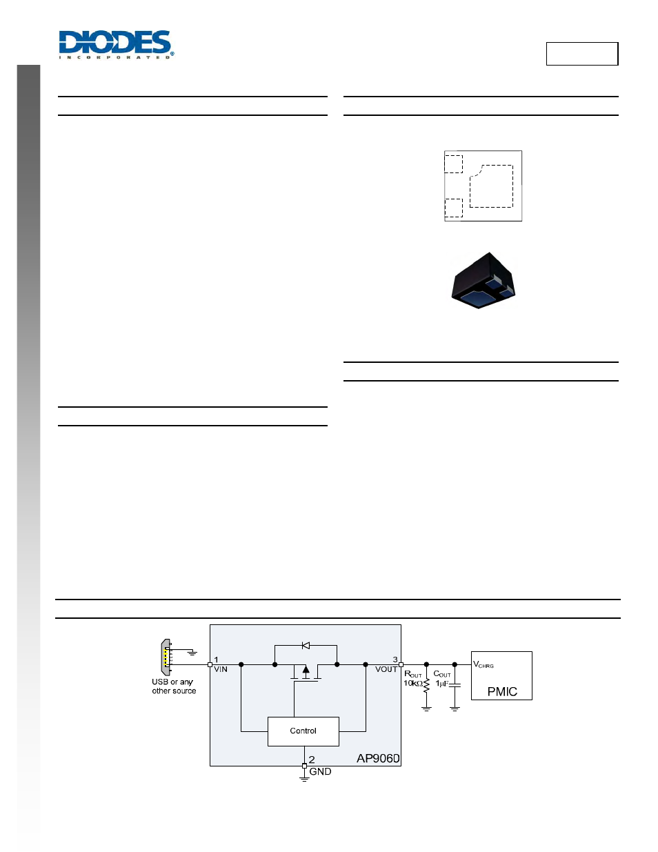
AP9060 is designed to protect the latest generation of PMICs for
portable applications such as Smartphones, UMPCs and others that
utilize battery power.
The device, with its integrated low resistance p-channel MOSFET,
operates as a switch and passes the input voltage through to the
output till the input reaches a clamp voltage limit. Once V
IN
goes
above the clamp limit, which is set to 11.15V, the output voltage gets
clamped and the feedback loop maintains the clamped V
OUT
by
reducing the drive to the p-channel FET.
The output voltage is clamped at 11.15V to ensure that a following
PMIC can detect a faulty charger and ensure safe and proper
communication to the system.
AP9060 also supports reverse operation whereby it can pass up to
1A of current from the PMIC to the load connected to the USB port.
This makes AP9060 suitable for USB On-The-Go enabled devices.
The AP9060 protection device is available in a low-profile
W-DFN1114-3 package with a typical height of 0.8mm.
Applications
•
Power Interface for New Generation PMICs
•
Charger Front-End Protection
• Smartphones
• UMPC
• Portable
Applications
Pin Assignments
W-DFN1114-3
2
3
1
Top View
Features
•
Wide Input Voltage Range of 3V – 30V
•
Ultra-Low Bias Current
•
Integrated Low On-Resistance P-Channel FET
•
Output Voltage Clamped at 11.15V
•
PMOS Protection Mechanism – Removes EMI Issues Typically
Associated with an NMOS Solution
•
Supports Reverse Current Operation (USB OTG)
•
Available in a W-DFN1114-3 Package
•
Totally Lead-Free & Fully RoHS Compliant (Notes 1 & 2)
•
Halogen and Antimony Free. “Green” Device (Note 3)
Notes:
1. No purposely added lead. Fully EU Directive 2002/95/EC (RoHS) & 2011/65/EU (RoHS 2) compliant.
2. Se information about Diodes Incorporated’s definitions of Halogen- and Antimony-free, "Green" and Lead-free.
3. Halogen- and Antimony-free "Green” products are defined as those which contain <900ppm bromine, <900ppm chlorine (<1500ppm total Br + Cl) and
<1000ppm antimony compounds.
Typical Applications Circuit
Figure 1 Typical Application Circuit