Ap6503, Application information – Diodes AP6503 User Manual
Page 9
AP6503
Document number: DS35077 Rev. 5 - 2
9 of 15
January 2013
© Diodes Incorporated
AP6503
Application Information
(cont.)
Over Voltage Protection
When the AP6503 FB pin exceeds 20% of the nominal regulation voltage of 0.925V, the over voltage comparator is tripped and the COMP pin
and the SS pin are discharged to GND, forcing the high-side switch off.
Thermal Shutdown
The AP6503 has on-chip thermal protection that prevents damage to the IC when the die temperature exceeds safe margins. It implements a
thermal sensing to monitor the operating junction temperature of the IC. Once the die temperature rises to approximately 160°C, the thermal
protection feature gets activated. The internal thermal sense circuitry turns the IC off thus preventing the power switch from damage.
A hysteresis in the thermal sense circuit allows the device to cool down to approximately +120°C before the IC is enabled again through soft
start. This thermal hysteresis feature prevents undesirable oscillations of the thermal protection circuit.
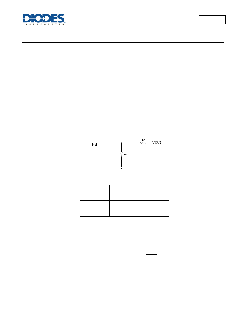
Setting the Output Voltage
The output voltage can be adjusted from 0.925V to 18V using an external resistor divider. Table 1 shows a list of resistor selection for common
output voltages. Resistor R1 is selected based on a design tradeoff between efficiency and output voltage accuracy. For high values of R1 there
is less current consumption in the feedback network. However the trade off is output voltage accuracy due to the bias current in the error
amplifier. R1 can be determined by the following equation:
⎟⎟
⎠
⎞
⎜⎜
⎝
⎛
−
⋅
=
1
0.925
V
R
R
OUT
2
1
Figure 3. Feedback Divider Network
When output voltage is low, network as shown in Figure 3 is recommended.
V
OUT
(V)
R1(KΩ) R2(KΩ)
5 45.3 10
3.3 26.1 10
2.5 16.9 10
1.8 9.53 10
1.2 3 10
Table 1
–
Resistor Selection for Common Output Voltages
Compensation Components
The AP6503 has an external COMP pin through which system stability and transient response can be controlled. COMP pin is the output of the
internal trans-conductance error amplifier. A series capacitor-resistor combination sets a pole-zero combination to control the characteristics of the
control system. The DC gain of the voltage feedback loop is given by:
OUT
V
FB
V
VEA
A
CS
G
LOAD
R
VDC
A
Ч
Ч
Ч
=
Where V
FB
is the feedback voltage (0.925V), R
LOAD
is the load resistor value, G
CS
is the current sense trans-conductance and A
VEA
is the error
amplifier voltage gain.