Ap6503, Absolute maximum ratings, Thermal resistance – Diodes AP6503 User Manual
Page 3: Recommended operating conditions
AP6503
Document number: DS35077 Rev. 5 - 2
3 of 15
January 2013
© Diodes Incorporated
AP6503
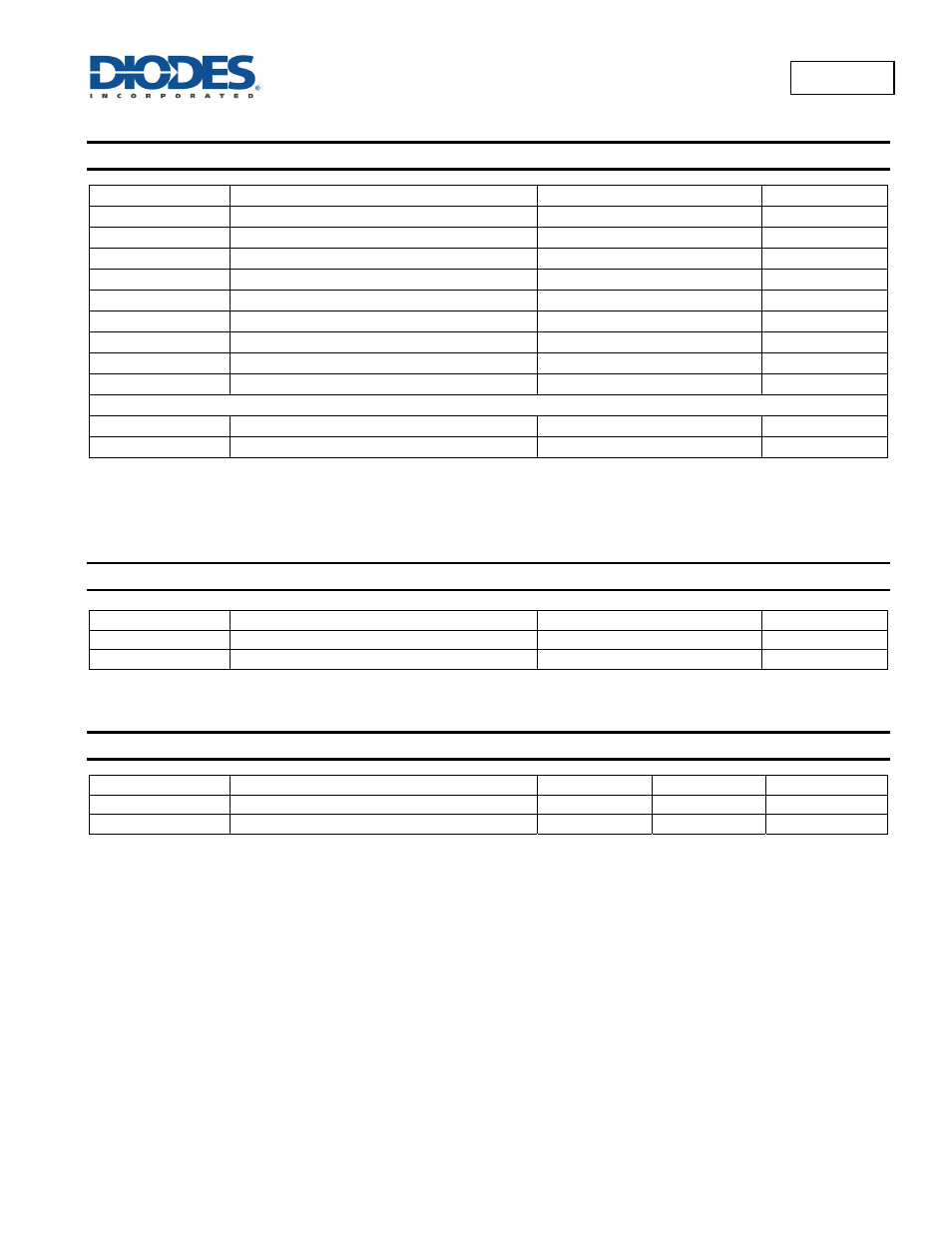
Absolute Maximum Ratings
(Note 4)
(@T
A
= +25°C, unless otherwise specified.)
Symbol Parameter
Rating
Unit
V
IN
Supply Voltage
-0.3 to +26
V
V
SW
Switch Node Voltage
-1.0 to V
IN
+0.3
V
V
BS
Bootstrap Voltage
V
SW
-0.3 to V
SW
+6
V
V
FB
Feedback Voltage
-0.3V to +6
V
V
EN
Enable/UVLO Voltage
-0.3V to +6
V
V
COMP
Comp Voltage
-0.3V to +6
V
T
ST
Storage Temperature
-65 to +150
°C
T
J
Junction Temperature
+150
°C
T
L
Lead Temperature
+260
°C
ESD Susceptibility (Note 5)
HBM
Human Body Model
3 kV
MM Machine
Model
250
V
Notes:
4. Stresses greater than the 'Absolute Maximum Ratings' specified above, may cause permanent damage to the device. These are stress ratings only;
functional operation of the device at these or any other conditions exceeding those indicated in this specification is not implied. Device reliability may
be affected by exposure to absolute maximum rating conditions for extended periods of time.
5. Semiconductor devices are ESD sensitive and may be damaged by exposure to ESD events. Suitable ESD precautions should be taken when
handling and transporting these devices.
Thermal Resistance
(Note 6)
Symbol Parameter
Rating
Unit
θ
JA
Junction to Ambient
74
°C/W
θ
JC
Junction to Case
16
°C/W
Note:
6. Test condition for SO-8EP: Measured on approximately 1” square of 1 oz copper
Recommended Operating Conditions
(Note 7)
(@T
A
= +25°C, unless otherwise specified.)
Symbol Parameter Min
Max
Unit
V
IN
Supply Voltage
4.7
23
V
T
A
Operating Ambient Temperature Range
-40
+85
°C
Note:
7. The device function is not guaranteed outside of the recommended operating conditions.