Ap6015, Block diagram, Absolute maximum ratings – Diodes AP6015 User Manual
Page 3
AP6015
High Efficiency Step-Down Low Power DC-DC Converter
AP6015 Rev. 3
3 of 18
FEBRUARY 2009
www.diodes.com
©
Diodes Incorporated
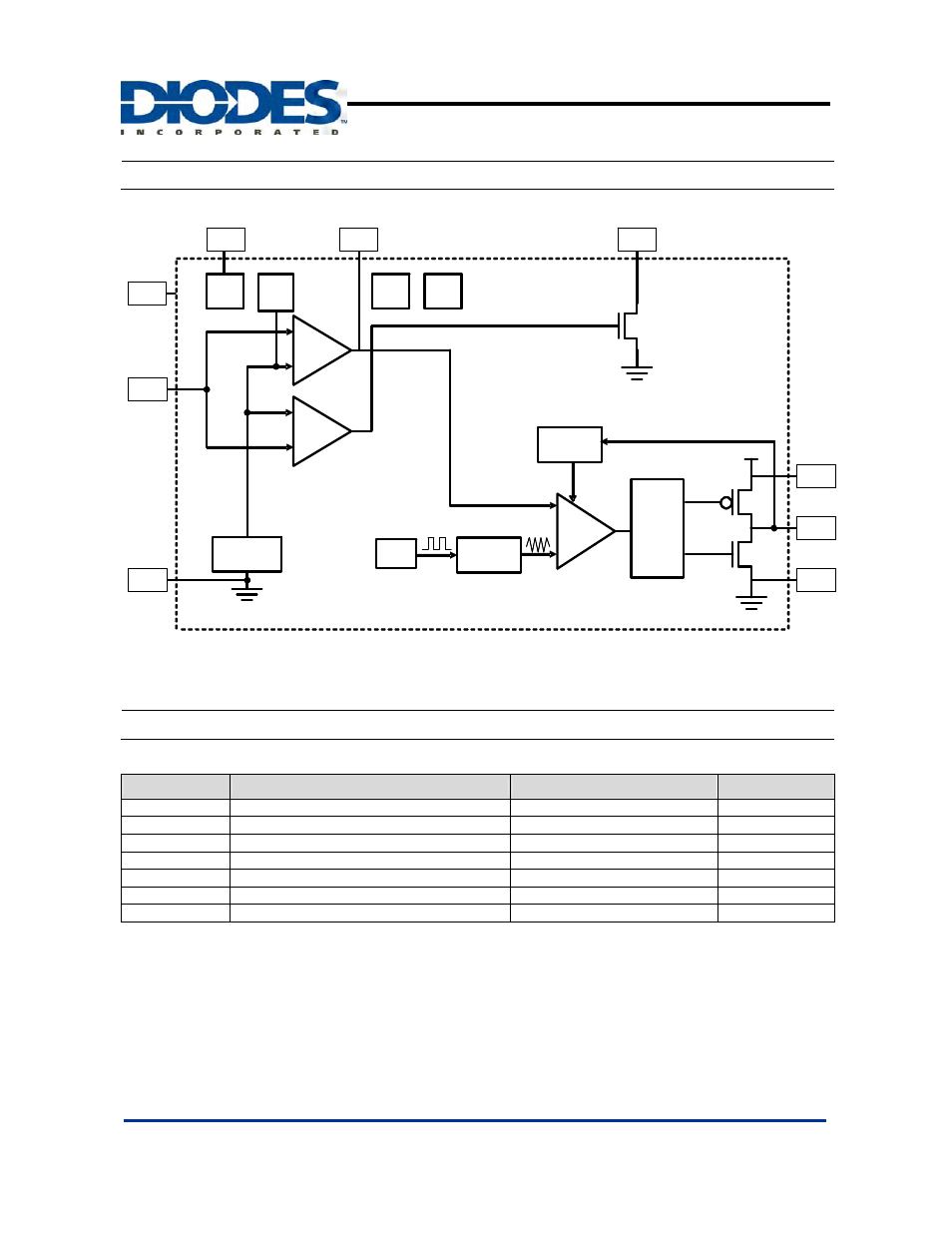
Block Diagram
+
-
PWM-COM
-
BANDGAP
Osc
Vramp
Current
Protection
-
+
ER-AMP
Buffer
-
+
PG_COM
UVLO
Open drain
TS
Bias
LX
FB
FB
PG
PG
CE
EN
CC
CC
PVCC
PGND
VCC
PGND
GND
PVCC
Vref=0.8V
SSSS
Notes: 3. The adjustable output voltage version does not use the internal feedback resistor divider.
The FB pin is directly connected to the error amplifier.
Absolute Maximum Ratings
Symbol
Parameter
Rating
Unit
ESD HBM
Human Body Model ESD Protection
2.5
KV
ESD MM
Machine Model ESD Protection
300
V
PVCC, VCC Supply Voltage
-0.3 to +5.5
V
Voltages on pins EN, CC, PG, FB, LX
-0.3 to V
IN
+0.3
V
T
J(MAX)
Maximum Junction Temperature Range
+150
o
C
T
ST
Storage temperature range
-65 to +150
o
C
T
OP
Operating Junction Temperature Range
-40 to +125
o
C
Stresses beyond those listed under “absolute maximum ratings” may cause permanent damage to the device. These are stress ratings only and functional
operation of the device at these or any other conditions beyond those indicated under “recommended operating conditions” is not implied. Exposure to
absolute-maximum-rated conditions for extended periods ma affect device reliability.