Ap6015, Application information – Diodes AP6015 User Manual
Page 16
AP6015
High Efficiency Step-Down Low Power DC-DC Converter
AP6015 Rev. 3
16 of 18
FEBRUARY 2009
www.diodes.com
©
Diodes Incorporated
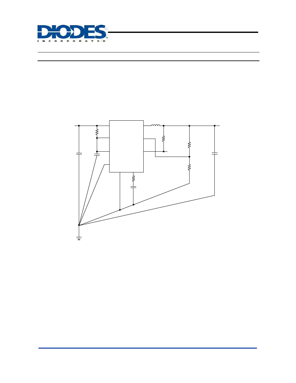
Layout Considerations
A good board layout practice can significantly improve the stability of the application circuit and reduce the
system noise. The feedback path must be as short as possible. The input capacitor and bypass capacitor
must be placed close to the PVCC and the VCC pins for optimal performance. It is recommended that the
ground planes for System Ground / Power Ground / Analog Ground are isolated from each others, while they
should all be joined together at a common point. An example drawing of a circuit with good ground noise
performance is shown below.
9
5
4
8
6
3
10
2
1
Power Good
C2
10 uF
C1
10µF
V
I
V
O
L1
LX
FB
PG
PGND
PVCC
EN
VCC
GND
CC
AP6015
R3
680K
R1
C
CC
100 pF
R2
1µF
100 Ohm
Rcc
C3
The external inductor must be placed as close as possible to the switching node, i.e. the LX pin. The copper
traces on the pcb, where high peak switching current may flow through, should be kept ‘wide’ and ‘short’.
This results in low inductance and capacitance in the current path, hence ground shift problem is avoided and
system stability stay within bound.
Application Information
(Continued)