Ap5100, Typical performance characteristics, Applications information – Diodes AP5100 User Manual
Page 7
AP5100
1.2A STEP-DOWN CONVERTER with 1.4MHz SWITCHING
FREQUENCY
AP5100
Document number: DS32130 Rev. 3 - 2
7 of 12
April 2012
© Diodes Incorporated
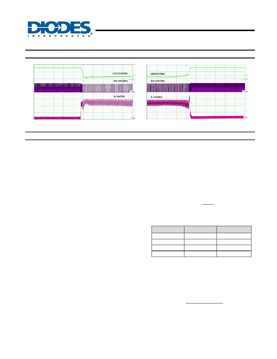
Typical Performance Characteristics
(cont.)
Short Circuit Entry
Short Circuit Recovery
Time- 50µs/div
Time- 100µs/div
Applications Information
OPERATION
The AP5100 is a current mode control, asynchronous buck
regulator. Current mode control assures excellent line and
load regulation and a wide loop bandwidth for fast
response to load transients. Figure. 4 depicts the
functional block diagram of AP5100.
The operation of one switching cycle can be explained as
follows. At the beginning of each cycle, HS (high-side)
MOSFET is off. The EA output voltage is higher than the
current sense amplifier output, and the current
comparator’s output is low. The rising edge of the 1.4MHz
oscillator clock signal sets the RS Flip-Flop. Its output
turns on HS MOSFET.
When the HS MOSFET is on, inductor current starts to
increase. The Current Sense Amplifier senses and
amplifies the inductor current. Since the current mode
control is subject to sub-harmonic oscillations that peak at
half the switching frequency, Ramp slope compensation is
utilized. This will help to stabilize the power supply. This
Ramp compensation is summed to the Current Sense
Amplifier output and compared to the Error Amplifier
output by the PWM Comparator. When the sum of the
Current Sense Amplifier output and the Slope
Compensation signal exceeds the EA output voltage, the
RS Flip-Flop is reset and HS MOSFET is turned off. The
external Schottky rectifier diode (D1) conducts the inductor
current.
For one whole cycle, if the sum of the Current Sense
Amplifier output and the Slope Compensation signal does
not exceed the EA output, then the falling edge of the
oscillator clock resets the Flip-Flop. The output of the
Error Amplifier increases when feedback voltage (VFB) is
lower than the reference voltage of 0.81V. This also
increases the inductor current as it is proportional to the
EA voltage.
Setting the Output Voltage
The output voltage can be adjusted from 0.81V to 15V
using an external resistor divider. Table 1 shows a list of
resistor selection for common output voltages. Resistor
R1 is selected based on a design tradeoff between
efficiency and output voltage accuracy. For high values of
R1 there is less current consumption in the feedback
network. However the trade off is output voltage accuracy
due to the bias current in the error amplifier. R2 can be
determined by the following equation:
⎟⎟
⎠
⎞
⎜⎜
⎝
⎛
−
×
=
1
0.81
OUT
V
2
R
1
R
Equation 1
V
OUT
(V)
R
1
(k
Ω)
R
2
(k
Ω)
1.8
80.6 (1%)
64.9 (1%)
2.5
49.9 (1%)
23.7 (1%)
3.3
49.9 (1%)
16.2 (1%)
5
49.9 (1%)
9.53 (1%)
Table 1. Resistor Selection for Common
Output Voltages
SW
f
L
ΔI
IN
V
)
OUT
V
IN
(V
OUT
V
L
Ч
Ч
−
Ч
=
Equation 2
Where
ΔI
L
is the inductor ripple current.
And f
SW
is the buck converter switching frequency.