Ap5100, Pin descriptions, Functional block diagram – Diodes AP5100 User Manual
Page 3
AP5100
1.2A STEP-DOWN CONVERTER with 1.4MHz SWITCHING
FREQUENCY
AP5100
Document number: DS32130 Rev. 3 - 2
3 of 12
April 2012
© Diodes Incorporated
Pin Descriptions
Pin Name
Pin #
Description
BST 1
Bootstrap. To form a boost circuit, a capacitor is connected between SW and BST pins to form a
floating supply across the power switch driver. This capacitor is needed to drive the power switch’s
gate above the supply voltage. Typical values for C
BST
range from 0.1µF to 1µF.
GND 2
Ground. This pin is the voltage reference for the regulated output voltage. All control circuits are
referenced to this pin. For this reason care must be taken in its layout.
FB 3
Feedback. To set the output voltage, connect this pin to the output resistor divider or directly to
V
OUT
. To prevent current limit run away during a current limit condition, the frequency foldback
comparator lowers the oscillator frequency when the FB voltage is below 400mV.
EN 4
On/Off Control Input. Do not leave this pin floating. To turn the device ON, pull EN above 1.2V and
to turn it off pull below 0.4V.
If enable/disable is not used, connect a 100k
Ω resistor between EN to V
IN
.
IN 5
Supply Voltage. The AP5100 operates from a +4.75V to +24V unregulated input. A decoupling
capacitor C1 is required to prevent large voltage spikes from appearing at the input. Place this
capacitor near the IC.
SW
6
Switch Output. This is the reference for the floating top gate driver.
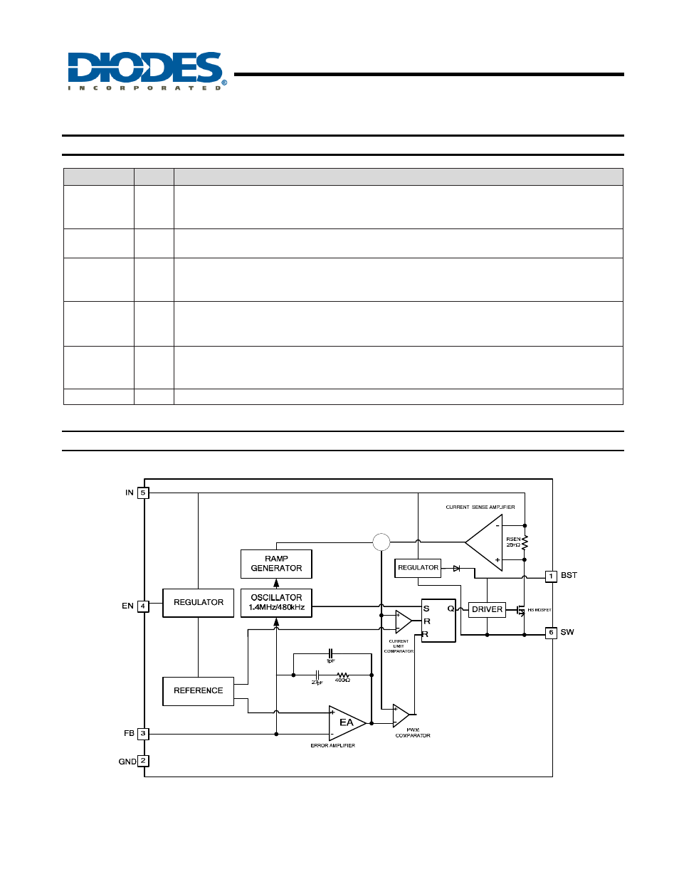
Functional Block Diagram
Σ
Figure 5. Functional Block Diagram