Ap3440 – Diodes AP3440 User Manual
Page 8
AP3440
Document number: DS36691 Rev. 2 - 2
8 of 15
March 2014
© Diodes Incorporated
AP3440
A Product Line of
Diodes Incorporated
N
E
W
P
R
O
D
U
C
T
Application Note
Theory of Operation
The AP3440 consists of a reference voltage module, slope compensation circuit, error amplifier, PWM comparator, current limit circuit, two N-
channel MOSFETs etc. (Refer to the Functional Block Diagram on page 3 for detailed information)
Soft-start
The AP3440 integrates an internal soft start circuit to minimize inrush currents or provide power supply sequencing during power up. A capacitor
connected between SS pin and ground implements the soft-start time. The AP3440 has an internal pull-up current source of 2
μA, which charges
the external slow start capacitor. Equation 1 calculates the required slow start capacitor, I
SS
is the internal slow start charging current of 2
μA, and
V
REF
is the internal voltage reference of 0.803V.
)
(
)
(
)
(
)
(
V
V
A
I
ms
t
nF
C
REF
SS
SS
SS
m
………………….(1)
During normal operation, if the V
IN
goes below the UVLO, or the EN pin is pulled below 1.2V, or a thermal shutdown occurs, the AP3440 will stop
switching and the SS pin will be discharged to 40mV before reinitiating a powering up sequence.
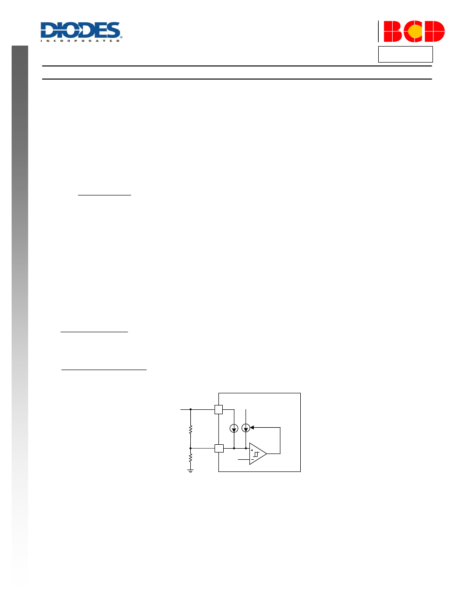
Enable and Adjusting UVLO
The AP3440 are disabled when the V
IN
falls below 2.6V. If an application requires a higher under-voltage lockout (UVLO), use the EN pin as
shown in Figure 1
to adjust the input voltage UVLO by using two external resistors. The EN pin has an internal pull-up current source that provides
the default condition of the AP3440 operating when the EN pin floats. Once the EN pin voltage exceeds 1.25V, an additional 2.55
μA of hysteresis
is added. When the EN pin is pulled below 1.18V, the 2.55
μA hysteresis is removed. This additional current facilitates input voltage hysteresis.
For AP3440, the divider resistor R1 and R2 on the EN pin can be calculated according to equation 2 and 3.
6
10
59
.
2
944
.
0
1
STOP
START
V
V
R
…………………...(2)
6
10
2
.
3
1
18
.
1
1
18
.
1
2
R
V
R
R
STOP
………………(3)
AP3440
R1
R2
VIN
EN
2.55
μA
0.6
μA
Figure 1. Adjustable Under Voltage Lock Out
Adjusting Output Voltage
The output voltage is set with a resistor divider from the FB pin. It is recommended to use divider resistors with 1% tolerance or better. Start with a
10k
Ω R2 resistor and use the equation 4 to calculate R1. To improve efficiency at very light loads consider using larger value resistors. If the
values are too high, the regulator is more susceptible to noise and voltage errors from the FB input current are noticeable.