Ap3440 – Diodes AP3440 User Manual
Page 10
AP3440
Document number: DS36691 Rev. 2 - 2
10 of 15
March 2014
© Diodes Incorporated
AP3440
A Product Line of
Diodes Incorporated
N
E
W
P
R
O
D
U
C
T
Application Note
(Cont.)
Over Current Protection
The AP3440 implements a cycle-by-cycle current limit. The high side switch current is detected during each cycle. During SCP conditions, V
OUT
is
pulled down and V
COMP
is drived to high, increasing the switch current. When the increased high side switch current is continuously detected to
trigger the current limit of high side switch 6 times, the high side and low side switches are turned off for about 2.5ms. Then both switches start
switching and they will not be turned off until the next 6 OCPs are triggered. The IC works with a hiccup mode during SCP conditions.
Power Good
The PGD pin output is an open drain MOSFET. The output is pulled low when the FB voltage enters the fault condition by falling below 91% or
rising above 107% of the nominal internal reference voltage. There is a 2% hysteresis on the threshold voltage, so when the FB voltage rises to
the good condition above 93% or falls below 105% of the internal voltage reference the PGD output MOSFET is turned off. It is recommended to
use a pull-up resistor between the values of 1k
Ω
Ω to a voltage source that is 5V or less. The PGD is in a valid state once the VIN input
voltage is greater than 1.2V.
Thermal Shutdown
The AP3440 implement an internal thermal shutdown to protect itself if the junction temperature exceeds +140°C. Switching is stopped when the
junction temperature exceeds the thermal trip threshold. Once the die temperature decreases below +120°C, the device reinitiates the soft start
operation. The thermal shutdown hysteresis is +20°C.
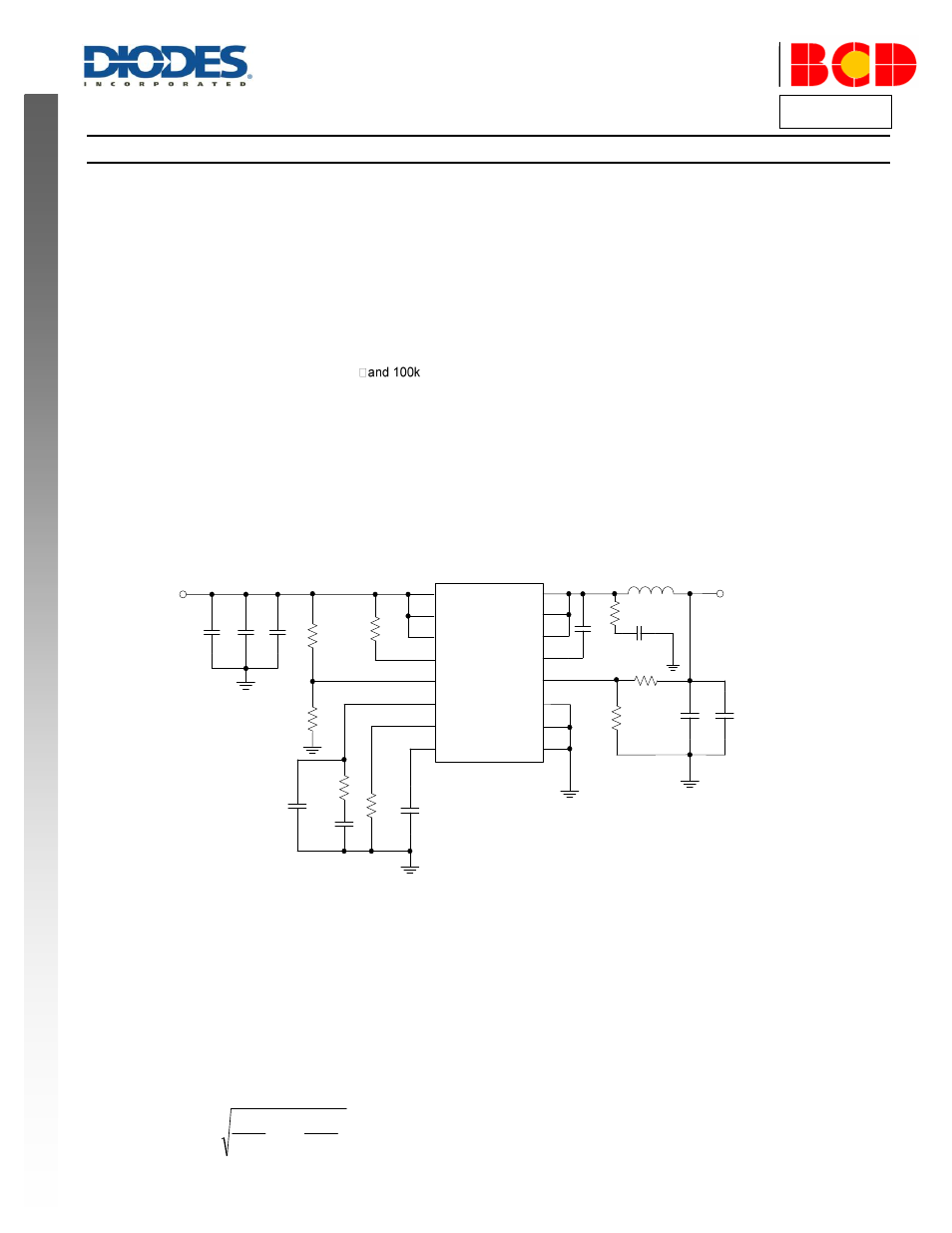
Component Selection
Typical application circuit of AP3440 is shown in Figure 5. For the major component selection please refer to the following section.
VIN
VIN
VIN
PGD
EN
COMP
SS
RT/CLK
SW
SW
SW
BOOT
FB
GND
GND
AGND
L1 1.5
m
H
V
OUT
=1.8V
R6 12.5k
Ω
R7
10k
Ω
V
IN
=5V
R4
100k
Ω
16
1
2
14
15
7
8
9
10
11
12
13
6
4
5
3
C5
Optional
C2
C7
0.01
m
F
C4
2.7nF
R3
7.5k
Ω
R5
180k
Ω
R1
R2
AP3440
C3
C9
22
m
F
C1
Optional
10
m
F 0.1
m
F
C8
22
m
F
U1
C6
0.1
m
F
R8 2.2
Ω
(Optional)
C10 2.2nF
(Optional)
Figure 5. Typical Application of AP3440
Input Capacitor
The AP3440 requires a high quality ceramic, type X5R or X7R, input decoupling capacitor of at least 4.7
μF effective capacitance and in some
applications a bulk capacitor. The effective capacitance includes any DC bias effects. To ensure a stable operation, the input capacitor should be
placed as close to the VIN pin as possible, and its value varies according to different load and different characteristic of input impedance.
There are two important parameters of the input capacitor: the voltage rating and RMS current rating. The voltage rating of the input capacitor
should be at least 1.25 times larger than the maximum input voltage. The capacitor must also have a RMS current rating greater than the
maximum input current ripple of the AP3440. The RMS current of input capacitor can be expressed as:
IN
OUT
IN
OUT
OUT(MAX)
CIN_RMS
V
V
1
V
V
I
I
………..(7)