Ap3591, Pin descriptions – Diodes AP3591 User Manual
Page 3
AP3591
Document number: DS36906 Rev.
1 - 2
3 of 18
March 2014
© Diodes Incorporated
AP3591
N
E
W
P
R
O
D
U
C
T
A Product Line of
Diodes Incorporated
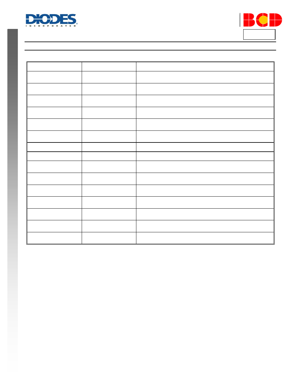
Pin Descriptions
Pin Number
Pin Name
Function
1
EN/DEM
Enable/Diode Emulation Mode control input. Connect to VDD for DEM mode;
connect to GND for shutdown and float the pin for CCM mode
2
TON
On time/Frequency adjustment pin. Connect to PHASE through a resistor. TON
is an input for the PWM controller
3
VOUT
Output voltage pin. Connect to the output of PWM converter. VOUT is an input
for the PWM controller
4
VDD
Analog supply voltage input for the internal analog integrated circuit. Bypass to
GND with a 1µF ceramic capacitor
5
FB
Feedback input pin. Connect FB pin to a resistor voltage divider from VOUT to
GND to adjust V
OUT
from 0.75V to 3.3V
6
PGOOD
Power good signal open-drain output for PWM converter. This pin will be pulled
high when the output voltage is within the target range
7
GND
Analog Ground
8
PGND
Power Ground
9
LGATE
Low-side N-MOSFET gate driver output for the PWM converter. This pin swings
between PGND and VDDP
10
VDDP
VDDP is the gate driver supply for external MOSFETs. Bypass to GND with a
1µF ceramic capacitor
11
CS
Over current trip point set input. Connect a resistor from this pin to signal ground
to set threshold for both over current limit and negative over current limit
12
PHASE
The UGATE High-side gate driver return. Also serves as anode of over current
comparator
13
UGATE
High-side N-MOSFET floating gate driver output for the PWM converter. This pin
swings between PHASE and BOOT
14
BOOT
Bootstrap pin. A bootstrap capacitor is connected for PWM converter. Connect
to an external ceramic capacitor to PHASE
–
Exposed Pad
The exposed pad must be soldered to a large PCB and connected to GND for
maximum power dissipation