Ap3591, Application information – Diodes AP3591 User Manual
Page 12
AP3591
Document number: DS36906 Rev.
1 - 2
12 of 18
March 2014
© Diodes Incorporated
AP3591
N
E
W
P
R
O
D
U
C
T
A Product Line of
Diodes Incorporated
Application Information
(Cont.)
Power On from EN (DEM Mode)
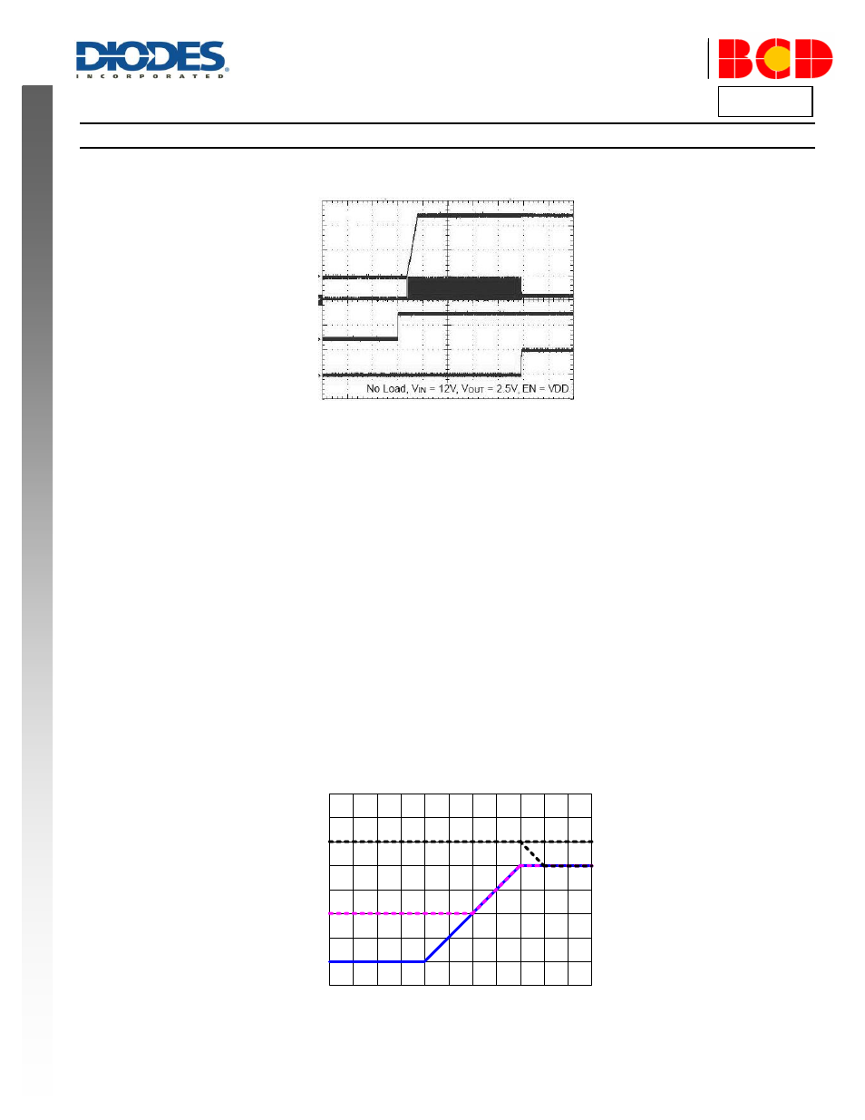
Figure 1. Start-up Behavior of AP3591
4. Power Good Output
The AP3591 features power good output to monitor the output voltage. It is an open-drain output and should be connected to a 5V power supply
node through a resistor. The power good function is active after the soft start is finished. PGOOD signal becomes high if output voltage reaches
±5% of the target value after 64µs delay building into the PGOOD circuitry. It will become low immediately if the output voltage goes beyond ±10%
of the target value.
5. Soft Stop
The AP3591 has a built in soft-stop circuitry. The output is discharged with an i
nternal 20Ω transistor when EN/DEM is low or the device is in a
fault condition including UVLO and OTP. The discharge time constant is determined by the output capacitance and resistance of the discharge
transistor.
6. Pre-biased Output
Figure 2 shows the normal V
OUT
start-up curve in blue; Initialization begins at T0, and output ramps between T1 and T2. If the output is pre-biased
to a voltage less than the expected value, as shown by the magenta curve, the AP3591 will detect that condition. Neither MOSFET will turn on
until the soft-start ramp voltage exceeds the output. V
OUT
starts seamlessly ramping from there. If the output is pre-biased to a voltage above the
expected value, as showed in the black curve, neither MOSFET will turn on until the output voltage is pulled down to the expected value through
external load. Any resistive load connected to the output will help pull down the voltage.
T0
T1
T2
V
OUT
Normal
V
OUT
Pre- Biased
V
OUT
Over-Charged
GND
Figure 2. Start-up Behavior with Pre-biased Output Voltage
V
OUT
1V/div
V
UGATE
20V/div
V
EN
2V/div
V
PGOOD
5V/div
Time 400µs/div