Pin descriptions, Functional block diagram – Diodes AP3968/69/70 User Manual
Page 3
AP3968/69/70
Document number: DS36759 Rev. 2 - 2
3 of 15
December 2013
© Diodes Incorporated
AP3968/69/70
A Product Line of
Diodes Incorporated
Pin Descriptions
Pin Number
Pin Name
Function
SO-7/PDIP-7
PDIP-8
1
1
CPC
This pin connects a capacitor to GND for output cable compensation
2
2
FB
The voltage feedback from auxiliary winding
3
3
VCC
This pin receives rectified voltage from the auxiliary winding of the transformer
4
4
CS
Current sense for primary side of transformer
5, 6
5, 6
C
This pin is connected with an internal power BJT’s collector
–
7
NC
Not connected
7
8
GND
This pin is the signal reference ground
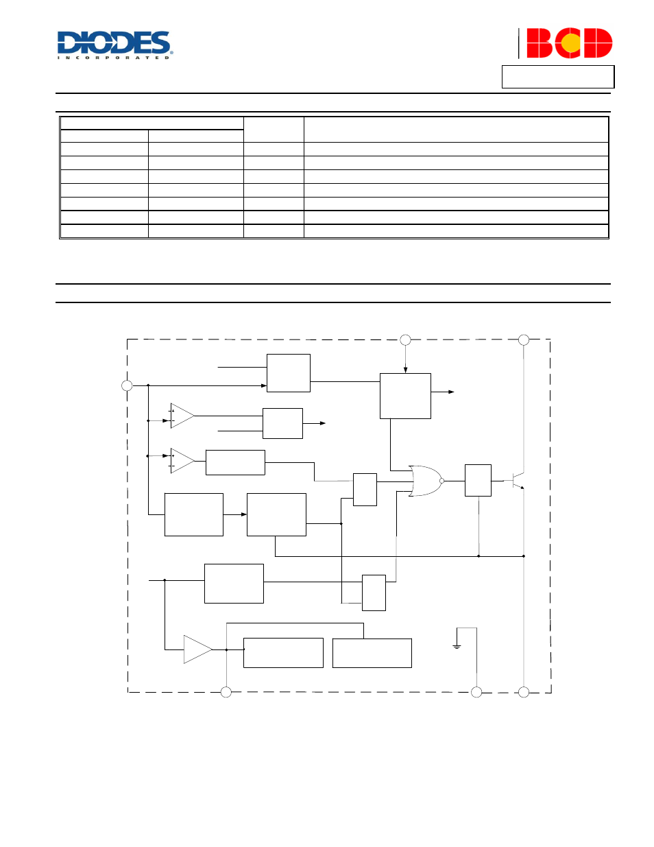
Functional Block Diagram
Regulator
&
Bias
OVP
&
OCkP
0.1V
V
FB
pfm
Tons
UVLO
COMP
EA
UVLO
CV_ctrl
pfm
Driver
R
Q
S
R
Q
S
Tons
CC_ctrl
FB
CS
CPC
VCC
C
GND
Cable Drop
Compensation
Constant
Voltage
Peak
Current
Control&
LEB
Constant
Current Control
Tonsec
Detector
Line Voltage
Compensation
Audible
Noise
Suppression
Buffer
1 (1)
2 (2)
3 (3)
4 (4)
5,6 (5,6)
7 (8)
A(B)
A for SO-7/PDIP-7
B for PDIP-8