Bsp75n, Application information, Minimum copper area characteristics – Diodes BSP75N User Manual
Page 5
BSP75N
© Zetex Semiconductors plc 2006
Application information
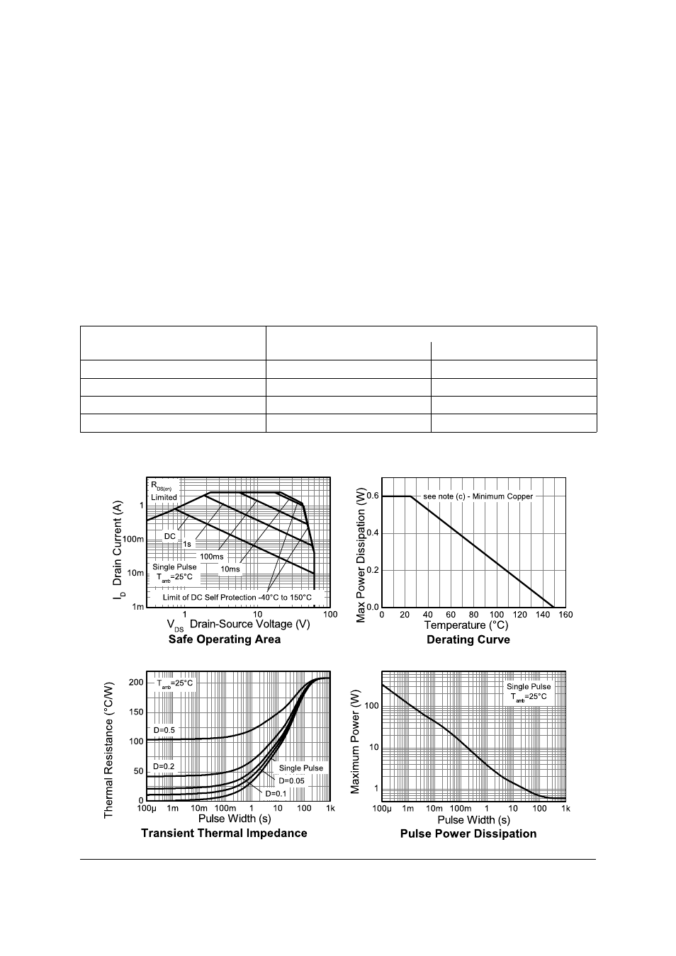
The current-limit protection circuitry is designed to de-activate at low V
DS
to prevent the load
current from being unnecessarily restricted during normal operation. The design max DC
operating current is therefore determined by the thermal capability of the package/board
combination, rather than by the protection circuitry (see graph on page 7 'Typical Output
Characteristic'). This does not compromise the products ability to self protect at low V
DS
.
The overtemperature protection circuit trips at a minimum of 150°C. So the available package
dissipation reduces as the maximum required ambient temperature increases. This leads to the
following maximum recommended continuous operating currents.
Minimum copper area characteristics
For minimum copper condition as described in note (c)
Max. ambient temperature T
amb
Maximum continuous current
V
IN
= 5V
V
IN
= 10V
25°C @ V
IN
= 5V
720
840
70°C @ V
IN
= 5V
575
670
85°C @ V
IN
= 5V
520
605
125°C @ V
IN
= 5V
320
375