Electrical characteristics, Switching characteristics – Diodes ULN200xA User Manual
Page 5
ULN2002A/ ULN2003A/ ULN2004A
Document number: DS35313 Rev. 5 - 2
5 of 11
June 2014
© Diodes Incorporated
ADVAN
CE I
N
F
O
RM
ATI
O
N
ULN2002A/ ULN2003A/ ULN2004A
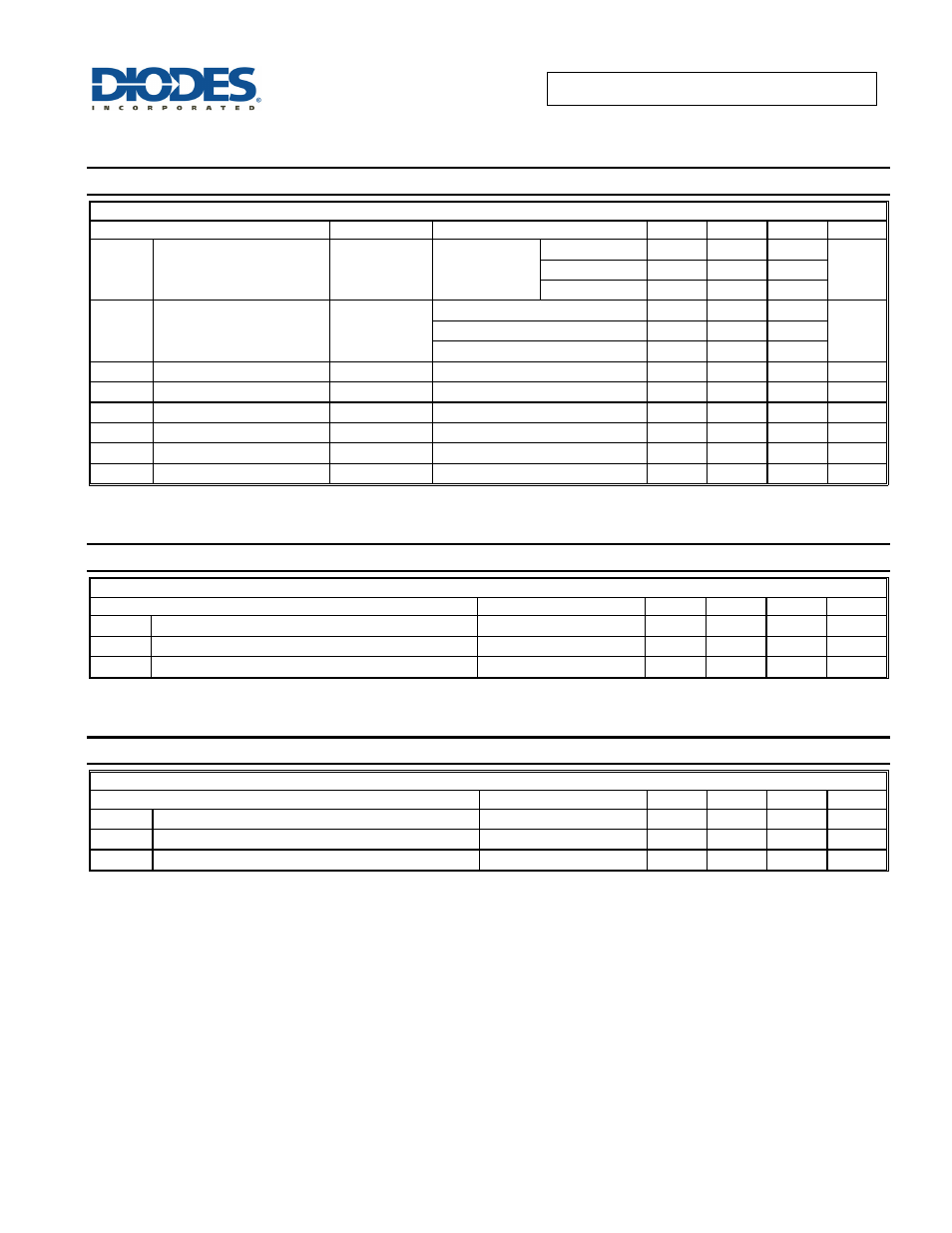
Electrical Characteristics
(@T
A
= -40°C to +105°C, unless otherwise specified.)
ULN2003A
Parameter Test
Figure
Test
Conditions
Min
Typ
Max
Unit
V
I(on)
On State Input Voltage
6
V
CE
= 2V
I
C
= 200mA
— — 2.7
V
I
C
= 250mA
— — 2.9
I
C
= 300mA
— — 3
V
CE(sat)
Collector Emitter Saturation
Voltage
5
I
I
= 250µA, I
C
= 100mA
— 0.9 1.2
V
I
I
= 350µA, I
C
= 200mA
— 1 1.4
I
I
= 500µA, I
C
= 350mA
— 1.2 1.7
V
F
Clamp Forward Voltage
8
I
F
= 350mA
— 1.7 2.2 V
I
CEX
Collector Cut-Off Current
1
V
CE
= 50V, I
I
= 0
— — 100 µA
I
I(off)
Off State Input Current
3
V
CE
= 50V, I
C
= 500µA
30 65 — µA
I
I
Input Current
4
V
I
= 3.85V
— 0.93 1.35 mA
I
R
Clamp Reverse Current
7
V
R
= 50V
— — 100 µA
C
I
Input Capacitance
—
V
I
= 0, f = 1MHz
— 15 25 pF
Switching Characteristics
(@T
A
= +25°C, unless otherwise specified.)
ULN2002A, ULN2003A, ULN2004A
Parameter Test
figure
Min
Typ
Max
Unit
t
PLH
Propagation delay time, low to high level output
10
—
0.25 1 µs
t
PLL
Propagation delay time, high to low level output
10
—
0.25 1 µs
V
OH
High level output voltage after switching
10 (V
S
= 50V, I
O
= 300mA)
V
S
-20
— — mV
Switching Characteristics
(@T
A
= -40 to +105°C, unless otherwise specified.)
ULN2003A
Parameter Test
figure
Min
Typ
Max
Unit
t
PLH
Propagation delay time, low to high level output
10
—
1 10 µs
t
PLL
Propagation delay time, high to low level output
10
—
1 10 µs
V
OH
High level output voltage after switching
10 (V
S
= 50V, I
O
= 300mA)
V
S
-50
— — mV