Absolute maximum ratings, Recommended operating conditions, Electrical characteristics – Diodes ULN200xA User Manual
Page 3
ULN2002A/ ULN2003A/ ULN2004A
Document number: DS35313 Rev. 5 - 2
3 of 11
June 2014
© Diodes Incorporated
ADVAN
CE I
N
F
O
RM
ATI
O
N
ULN2002A/ ULN2003A/ ULN2004A
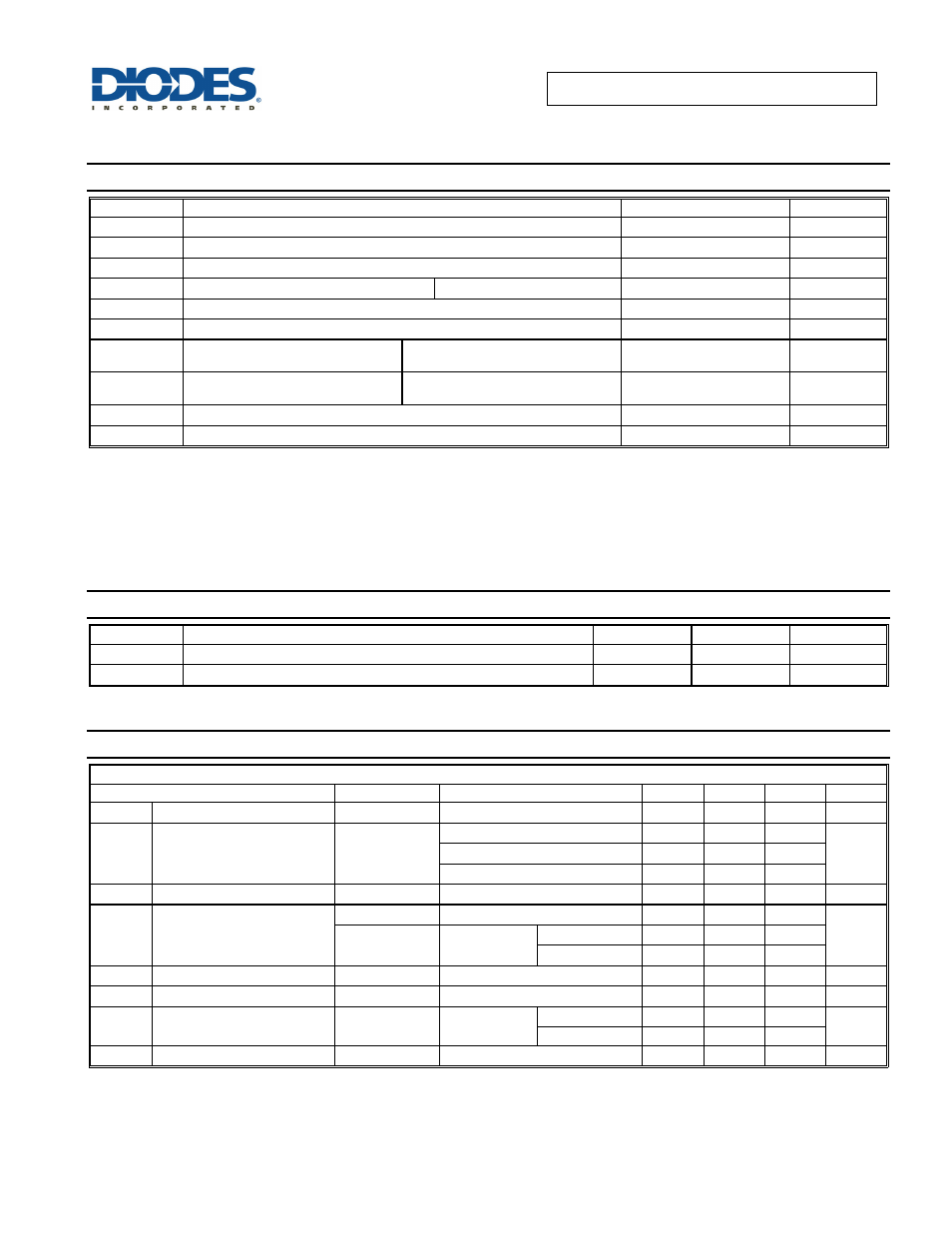
Absolute Maximum Ratings
(Note 4)
(@T
A
= +25°C, unless otherwise specified.)
Symbol Parameter
Rating
Unit
V
CC
Collector to Emitter Voltage
50
V
V
R
Clamp Diode Reverse Voltage (Note 5)
50
V
V
I
Input Voltage (Note 5)
30
V
I
CP
Peak Collector Current
See Typical Characteristics
500
mA
I
OK
Output Clamp Current
500
mA
I
TE
Total Emitter Current
-2.5
A
θ
JA
Thermal Resistance Junction-to-
Ambient (Note 6)
SO-16 63.0
°C/W
θ
JC
Thermal Resistance Junction-to-Case
(Note 6)
SO-16 12.0
°C/W
T
J
Junction Temperature
+150
°C
T
STG
Storage Temperature
-65 to +150
°C
Notes: 4. Stresses beyond those listed under "absolute maximum ratings" may cause permanent damage to the device. These are stress ratings only.
Functional operation of the device at these or any other conditions beyond those indicated under "recommended operating conditions" is not
implied. Exposure to absolute-maximum-rated conditions for extended periods may affect device reliability.
5. All voltage values are with respect to the emitter/substrate terminal E, unless otherwise noted.
6. Maximum power dissipation is a function of T
J
(max), θ
JA
, and T
A
. The maximum allowable power dissipation at any allowable ambient temperature
is P
D
= (T
J
(max)
– T
A
)/θ
JA
. Operating at the absolute maximum T
J
of 150°C can affect reliability.
7. Maximum power dissipation is a function of T
J
(max), θ
JC
, and T
A
. The maximum allowable power dissipation at any allowable ambient temperature
is P
D
= (T
J(max)
– T
C
)/θ
JA
. Operating at the absolute maximum T
J
of 150°C can affect reliability.
Recommended Operating Conditions
Symbol Parameter
Min
Max
Unit
V
CC
Collector to Emitter voltage
—
50 V
T
A
Operating Ambient Temperature
-40
+105
°C
Electrical Characteristics
(@T
A
= +25°C, unless otherwise specified.)
ULN2002A
Parameter Test
Figure
Test
Conditions
Min
Typ
Max
Unit
V
I(on)
On State Input Voltage
6
V
CE
= 2V, I
C
= 300mA
— — 13 V
V
CE(sat)
Collector Emitter Saturation
Voltage
5
I
I
= 250µA, I
C
= 100mA
— 0.9 1.1
V
I
I
= 350µA, I
C
= 200mA
— 1 1.3
I
I
= 500µA, I
C
= 350mA
— 1.2 1.6
V
F
Clamp Forward Voltage
8
I
F
= 350mA
— 1.7 2 V
I
CEX
Collector Cut-Off Current
1
V
CE
= 50V, I
I
= 0
— — 50
µA
2
V
CE
= 50V,
T
A
= 105°C
I
I
= 0
— — 100
V
I
= 6V
— — 500
I
I(off)
Off State Input Current
3
V
CE
= 50V, I
C
= 500µA
50 65 — µA
I
I
Input Current
4
V
I
= 17V
— 0.82 1.25 mA
I
R
Clamp Reverse Current
7
V
R
= 50V
T
A
= +105°C
— — 100
µA
— —
—
50
C
I
Input Capacitance
—
V
I
= 0, f = 1MHz
— — 25 pF