New prod uc t zxbm5210, Functional block diagram, Absolute maximum ratings – Diodes ZXBM5210 User Manual
Page 3: Recommended operating conditions
ZXBM5210
Document number: DS36765 Rev. 1 - 2
3 of 17
December 2013
© Diodes Incorporated
NEW PROD
UC
T
ZXBM5210
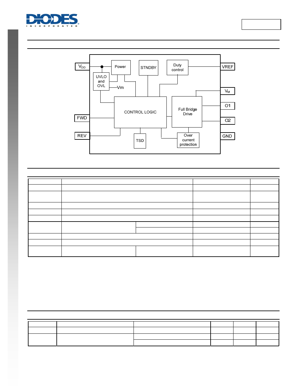
Functional Block Diagram
Absolute Maximum Ratings
(Note 5) @T
A
= +25°C, unless otherwise specified.)
Symbol Characteristic
Values
Unit
V
M
and V
DD,
Supply voltage (Note 6)
24
V
V
OUT1,
V
OUT2
V
REF
All other pins except FWD and REV pins
24
V
V
FWD
and V
REV
FWD and REV pin voltage
7
V
V
REVERSE
Reverse supply Voltage on all pins
-0.3
V
I
OUTPUT
Output current (source and sink)- Peak
1500
mA
P
D
Package power dissipation
SO8 (Note 7)
1043
mW
SO8-EP (Note 8)
2980
mW
Ts
Storage temperature range
-65 to +150
°C
T
J
Maximum junction temperature
150
°C
ESD HBM
Human Body Model ESD withstand
capability
V
DD
, V
M
, V
REF
, FWD, REV,
GND and OUT1 OUT2 pins
6
kV
Notes:
5. Stresses greater than the 'Absolute Maximum Ratings' specified above, may cause permanent damage to the device. These are stress ratings
only; functional operation of the device at these or any other conditions exceeding those indicated in this specification is not implied. Device
reliability may be affected by exposure to absolute maximum rating conditions for extended periods of time
6. The absolute maximum supply voltage of 24V is a transient stress rating and is not meant as a functional operating condition. It is not recommended
to operate the device at the absolute maximum rated conditions for any period of time.
7. SO-8 soldered to minimum recommended landing pads (see Package Outline Dimension section) on a 1”x1” two-layer 2oz.copper FR4 PCB
(1.6mm thickness) without any via or copper flood on the bottom layer. See thermal de-rating curves in the thermal performance section.
8. SO-8EP exposed pad soldered to minimum recommended landing pads (see Package Outline Dimension section) on a 2”x2” two-layer 2oz.copper
FR4 PCB (1.6mm thickness) with four thermal vias in the exposed PAD to the copper flood on the bottom layer. See thermal de-rating curves in the
thermal performance section.
Recommended Operating Conditions
Symbol Characteristic
Conditions Min
Max
Unit
V
DD
Supply Voltage
Operating
3
18
V
T
A
Operating Temperature Range
Operating, SO8 package
-40
+85
°C
Operating, SO8-EP package
-40
+105
°C