New prod uc t zxbm5210, Typical applications circuit, Pin descriptions – Diodes ZXBM5210 User Manual
Page 2
ZXBM5210
Document number: DS36765 Rev. 1 - 2
2 of 17
December 2013
© Diodes Incorporated
NEW PROD
UC
T
ZXBM5210
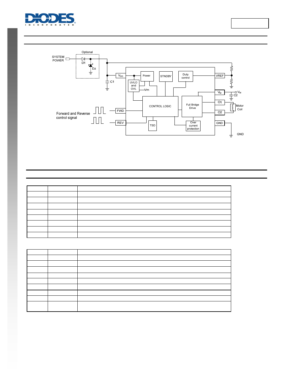
Typical Applications Circuit
Note:
4. C1 is for power stabilization and to strengthen the noise immunity, the recommended capacitance is 100nF to 1µF or more.
C2 is a re-circulating capacitor for back rush voltage and recommended capacitance is 100nF for low current applications to 10µF or more for large
current applications. See application note section
Pin Descriptions
Package: SO-8
Pin #
Pin Name
Function
1
OUT1
Driver output
2
V
M
Power Supply Voltage
3
V
DD
Power Supply Voltage
4
FWD
Forward Control Input (logic level, 5.5V max)
5
REV
Reverse Control Input (logic level, 5.5V max)
6
V
REF
Input reference voltage to set the internal PWM oscillator duty ratio
7 OUT2
Driver
Output
8 GND
Ground
Package: SO8-EP
Pin #
Pin Name
Function
1
OUT1
Driver output
2
V
M
Power Supply Voltage
3
V
DD
Power Supply Voltage
4
FWD
Forward Control Input (logic level, 5.5V max)
5
REV
Reverse Control Input (logic level, 5.5V max)
6
V
REF
Input reference voltage to set the internal PWM oscillator duty ratio
7 OUT2
Driver
Output
8 GND
Ground
Pad Pad
The exposed pad is for thermal dissipation and it is internally connected to the ground.
On the PCB layout, it can be connected to GND or left open circuit.