Zxsc400 – Diodes ZXSC400 User Manual
Page 4
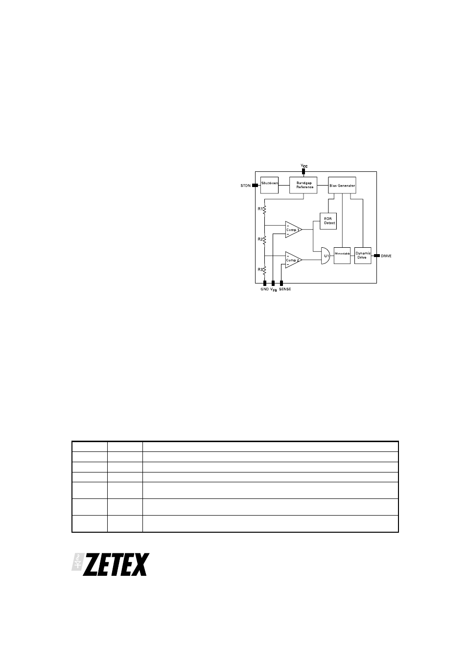
DESIGN INFORMATION
IC operation description
Bandgap Reference
All threshold voltages and internal currents are
derived from a temperature compensated bandgap
reference circuit with a reference voltage of 1.22V
nominal.
Dynamic Drive Output
Depending on the input signal, the output is either
“LOW” or “HIGH”. In the high state a 2.5mA current
source (max drive voltage = V
CC
-0.4V) drives the base
or gate of the external transistor. In order to operate
the external switching transistor at optimum
efficiency, both output states are initiated with a short
transient current in order to quickly discharge the base
or the gate of the switching transistor.
Switching Circuit
The switching circuit consists of two comparators,
Comp1 and Comp2, a gate U1, a monostable and the
drive output. Normally the DRIVE output is “HIGH”; the
external switching transistor is turned on. Current
ramps up in the inductor, the switching transistor and
external current sensing resistor. This voltage is
sensed by comparator, Comp2, at input I
SENSE
. Once
the current sense voltage across the sensing resistor
exceeds 30mV, comparator Comp2 through gate U1
triggers a re-triggerable monostable and turns off the
output drive stage for 2
s. The inductor discharges to
the load of the application. After 2
s a new charge
cycle begins, thus ramping the output voltage. When
the output voltage reaches the nominal value and FB
gets an input voltage of more than 300mV, the
monostable is forced “on” from Comp1 through gate
U1, until the feedback voltage falls below 300mV. The
above action continues to maintain regulation.
ZXSC400
ISSUE 1 - JANUARY 2003
4
Pin No.
Name
Description
1
V
CC
Supply voltage, 1.8V to 8V.
2
GND
Ground
3
STDN
Shutdown
4
SENSE
Inductor current sense input. Internal threshold voltage set to 30mV. Connect
external sense resistor
5
V
FB
Reference voltage. Internal threshold set to 300mV. Connect external resistor
to program LED current
6
DRIVE
Drive output for external switching transistor. Connect to base or gate of
external switching transistor.
Pin functions
2µs
Block diagram