Application information, Ti i – Diodes ZXSC410/ZXSC420/ZXSC440 User Manual
Page 7
ZXSC410/ZXSC420/ZXSC440
Document number: DS33618 Rev. 5 - 2
7 of 17
March 2013
© Diodes Incorporated
ZXSC410/ZXSC420/ZXSC440
Application Information
(cont.)
Output Power Calculation
By making the above assumptions for inductance and peak current the output power can be determined by:
P
OUT
= I
AV
x V
IN
x η = (Watts)
where
t
t
t
t
I
I
OFF
ON
DIS
ON
PK
AV
x
2
and
V
I
t
IN
PK
ON
xL
and
V
V
I
t
IN
IN
PK
DIS
xL
and
t
OFF
≈ 1.7μs (internally set by ZXSC410/420/440)
and
η = efficiency i.e. 100% = 1
Operating frequency can be derived by:
t
t
OFF
ON
1
f
Output Adjustment
The ZXSC410/420/440 are adjustable output controllers allowing the end user the maximum flexibilty. They can be used both as switching
voltage regulators and as constant current regulators. A feedback voltage of 300mV provides a good compromise for both voltage and current
regulation.
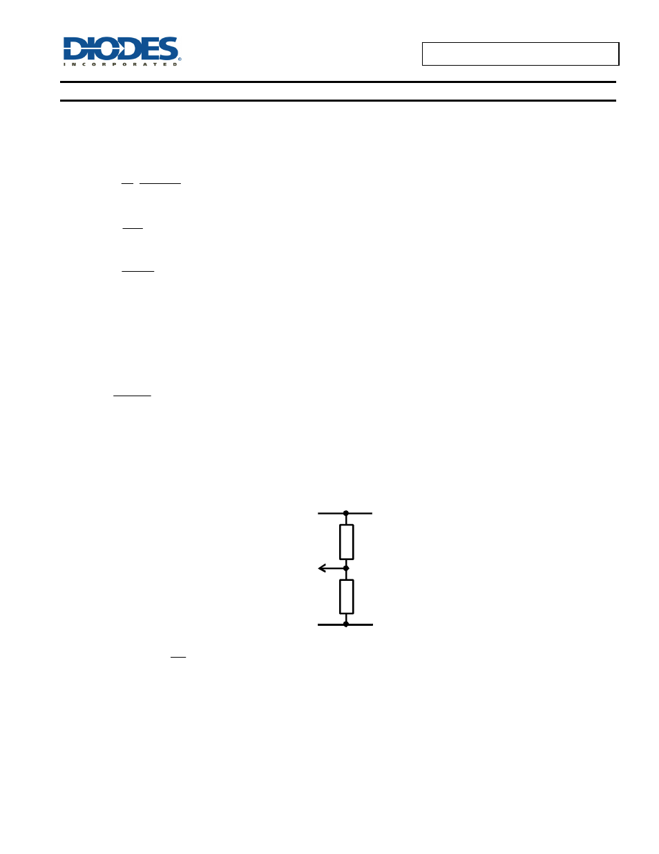
For a constant output voltage operation a potential divider network is connected as follows:
V
FB
V
OUT
GND
R
A
R
B
The output voltage is determined by the equation:
RB
RA
1
V
V
FB
OUT
where
V
FB
= 300mV
The resistor values, RA and RB, should be maximised to improve efficiency and decrease battery drain. Optimisation can be achieved by
providing a minimum current of I
FB(MAX)
= 200nA to the VFB pin. Output is adjustable from V
FB
to the (BR)V
CEO
of the switching transistor, Q1.
Note: For the reference designs, RA is assigned the label R2 and RB the label R3.
The ZXSC410/420/440 can also be used to generate a constant current between boosted output rail and the VFB pin by connecting a single
resistor between VFB and GND.