Pin descriptions, Functional block diagram – Diodes ZXSC410/ZXSC420/ZXSC440 User Manual
Page 2
ZXSC410/ZXSC420/ZXSC440
Document number: DS33618 Rev. 5 - 2
2 of 17
March 2013
© Diodes Incorporated
ZXSC410/ZXSC420/ZXSC440
Pin Descriptions
Pin Name
Pin Number
Function
ZXSC410 ZXSC420 ZXSC440
V
CC
1 1 8
Supply
Voltage
GND 2 2 7
Ground
STDN
3
—
5
Shutdown (ZXSC410 and ZXSC440)
EOR
—
3
6
End of regulation (ZXSC420 and ZXSC440)
Sense 4 4 3
Inductor current sense input. Internal threshold voltage set to 28mV.
Connect external sense resistor.
V
FB
5 5 2
Reference voltage. Internal threshold set to 300mV.
Connect external resistor network to set output voltage.
Drive 6 6 1
Drive output for external switching transistor.
Connect to base or gate of external switching transistor.
NC — — 4
No
connection
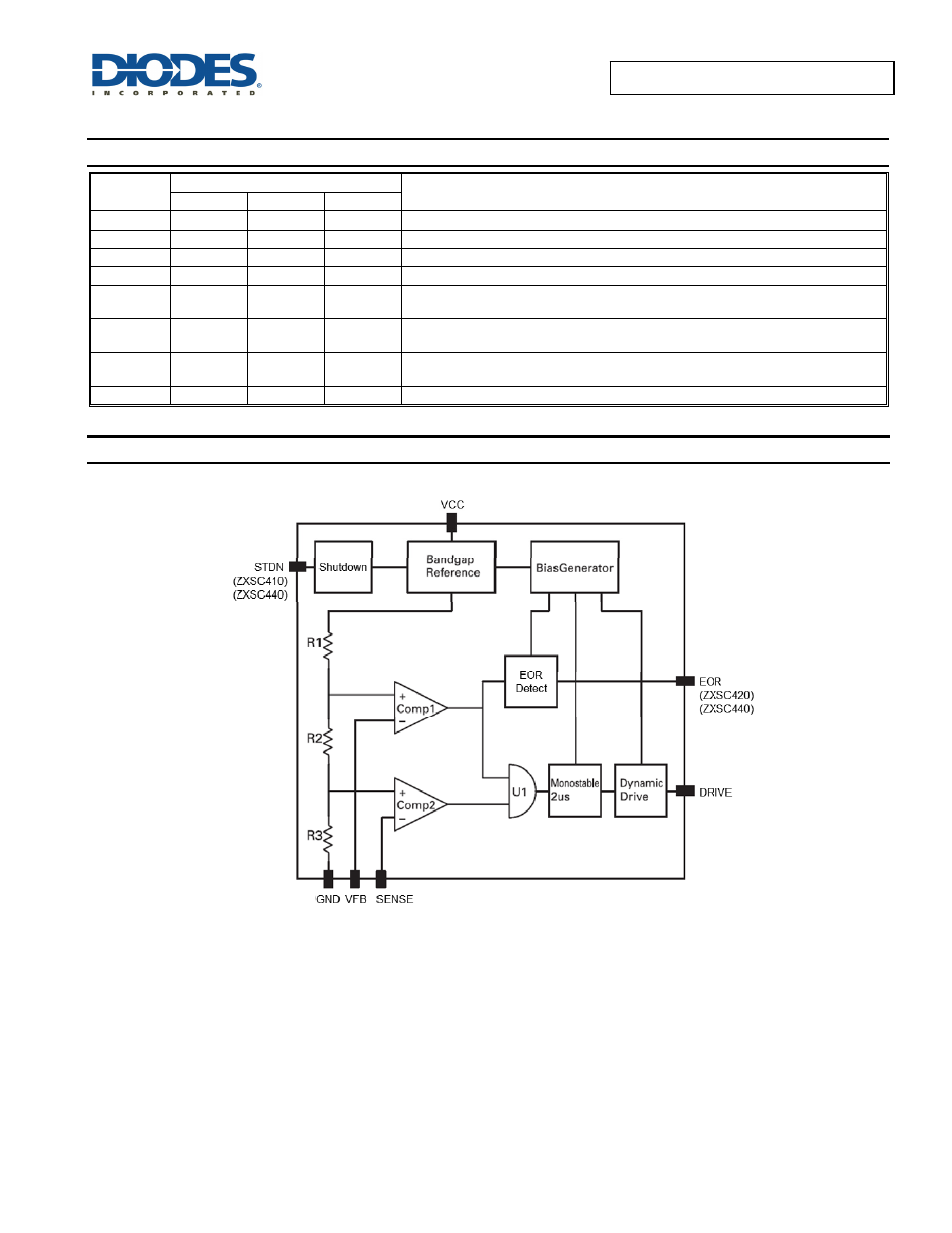
Functional Block Diagram
- PDS3200 (5 pages)
- PDS340 (5 pages)
- PDS340Q (5 pages)
- PDS360 (5 pages)
- PDS360Q (5 pages)
- PDS4150 (4 pages)
- PDS3100Q (5 pages)
- PDS3100 (5 pages)
- PDS1240CTL (5 pages)
- PDS1045 (5 pages)
- PDS1040L (5 pages)
- PDS1040CTL (5 pages)
- PDS1040 (5 pages)
- PD3S230L (5 pages)
- PD3S230H (3 pages)
- PDS5100Q (5 pages)
- PDS835L (5 pages)
- PDS760 (5 pages)
- PDS560 (5 pages)
- PDS540 (5 pages)
- PDS5100H (5 pages)
- PDS5100 (5 pages)
- PDS4200H (6 pages)
- SBL3060CTP (4 pages)
- SBL30L30CT (3 pages)
- SBL3045CTP (4 pages)
- SBL3040CTP (4 pages)
- SBL2060CTP (4 pages)
- SBL2030CT - SBL2060CT (3 pages)
- SBL2045CTP (4 pages)
- SBL1060CTP (4 pages)
- SBL1040CTP (4 pages)
- SBG3030CT - SBG3045CT (5 pages)
- SB520 - SB560 (3 pages)
- SB370 - SB3100 (3 pages)
- SB320 - SB360 (3 pages)
- SBR10U100CT (5 pages)
- SBR10U150CT (5 pages)
- SBR10A45SP5 (5 pages)
- SBR1060CT (5 pages)
- SBR1045SP5 (5 pages)
- SBR1045SD1 (4 pages)
- SBR1045D1 (5 pages)
- SBR1045CTL (4 pages)
- SBR1040CT (5 pages)