Maximum ratings, Thermal characteristics – Diodes ZXMS6006DT8 User Manual
Page 3
ZXMS6006DT8
Document number: DS35143 Rev. 1 - 2
3 of 9
December 2010
© Diodes Incorporated
ZXMS6006DT8
ADVAN
CE I
N
F
O
RM
ATI
O
N
A Product Line of
Diodes Incorporated
IntelliFET
®
is a trademark of Diodes Incorporated, registered in the United States and other jurisdictions worldwide.
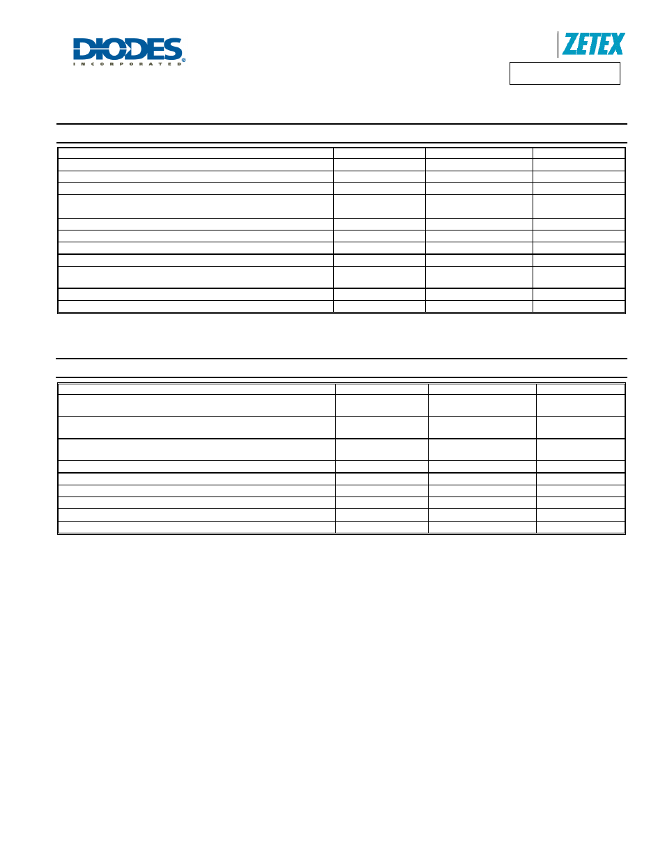
Maximum Ratings
@T
A
= 25°C unless otherwise specified
Characteristic Symbol
Value
Units
Continuous Drain-Source Voltage
V
DS
60 V
Drain-Source Voltage For Short Circuit Protection
V
DS(SC)
16 V
Continuous Input Voltage
V
IN
-0.5 ... +6
V
Continuous Input Current @-0.2V
IN
≤ 6V
Continuous Input Current @V
IN
< -0.2V or V
IN
> 6V
I
IN
No limit
│I
IN
│≤2
mA
Pulsed Drain Current @V
IN
= 3.3V ( Note 6)
I
DM
11 A
Pulsed Drain Current @V
IN
= 5V ( Note 6)
I
DM
13 A
Continuous Source Current (Body Diode) (Note 4)
I
S
2 A
Pulsed Source Current (Body Diode)
I
SM
12 A
Unclamped Single Pulse Inductive Energy,
T
J
= 25
°C, I
D
= 0.5A, V
DD
= 24V
E
AS
210 mJ
Electrostatic Discharge (Human Body Model)
V
ESD
4000 V
Charged Device Model
V
CDM
1000 V
Thermal Characteristics
@T
A
= 25°C unless otherwise specified
Characteristic Symbol
Value
Units
Power Dissipation at T
A
= 25
°C (Notes 4 & 7)
Linear Derating Factor
P
D
1.16
9.28
W
mW/
°C
Power Dissipation at T
A
= 25
°C (Notes 4 & 8)
Linear Derating Factor
P
D
1.67
13.3
W
mW/
°C
Power Dissipation at T
A
= 25
°C (Notes 5 & 7)
Linear Derating Factor
P
D
2.13
17
W
mW/
°C
Thermal Resistance, Junction to Ambient (Notes 4 & 7)
R
θJA
108
°C/W
Thermal Resistance, Junction to Ambient (Notes 4 & 8)
R
θJA
75
°C/W
Thermal Resistance, Junction to Case (Notes 5 & 7)
R
θJC
58.7
°C/W
Thermal Resistance, Junction to Case (Note 9)
R
θJC
26.5
°C/W
Operating Temperature Range
T
J
-40 to +150
°C
Storage Temperature Range
T
STG
-55 to +150
°C
Notes:
4. For a dual device surface mounted on a 25mm x 25mm single sided 1oz weight copper split down the middle on 1.6mm FR4 board, in still air conditions.
5. For a dual device surface mounted on FR4 PCB measured at t
≤ 10sec
6. Repetitive rating25mm x 25mm FR4 PCB, D = 0.02, Pulse width = 300µs – pulse width limited by junction temperature. Refer to transient thermal
impedance graph.
7. For a dual device with one active die.
8. For a dual device with 2 active die running at equal power.
9. Thermal resistance from junction to the mounting surface of the drain pin.