Maximum ratings, Thermal characteristics, Recommended operating conditions – Diodes ZXMS6005DT8 User Manual
Page 3
ZXMS6005DT8
Document number: DS32248 Rev. 2 - 2
3 of 9
March 2013
© Diodes Incorporated
ZXMS6005DT8
ADVAN
CE I
N
F
O
RM
ATI
O
N
IntelliFET
®
is a trademark of Diodes Incorporated, registered in the United States and other jurisdictions worldwide.
A Product Line of
Diodes Incorporated
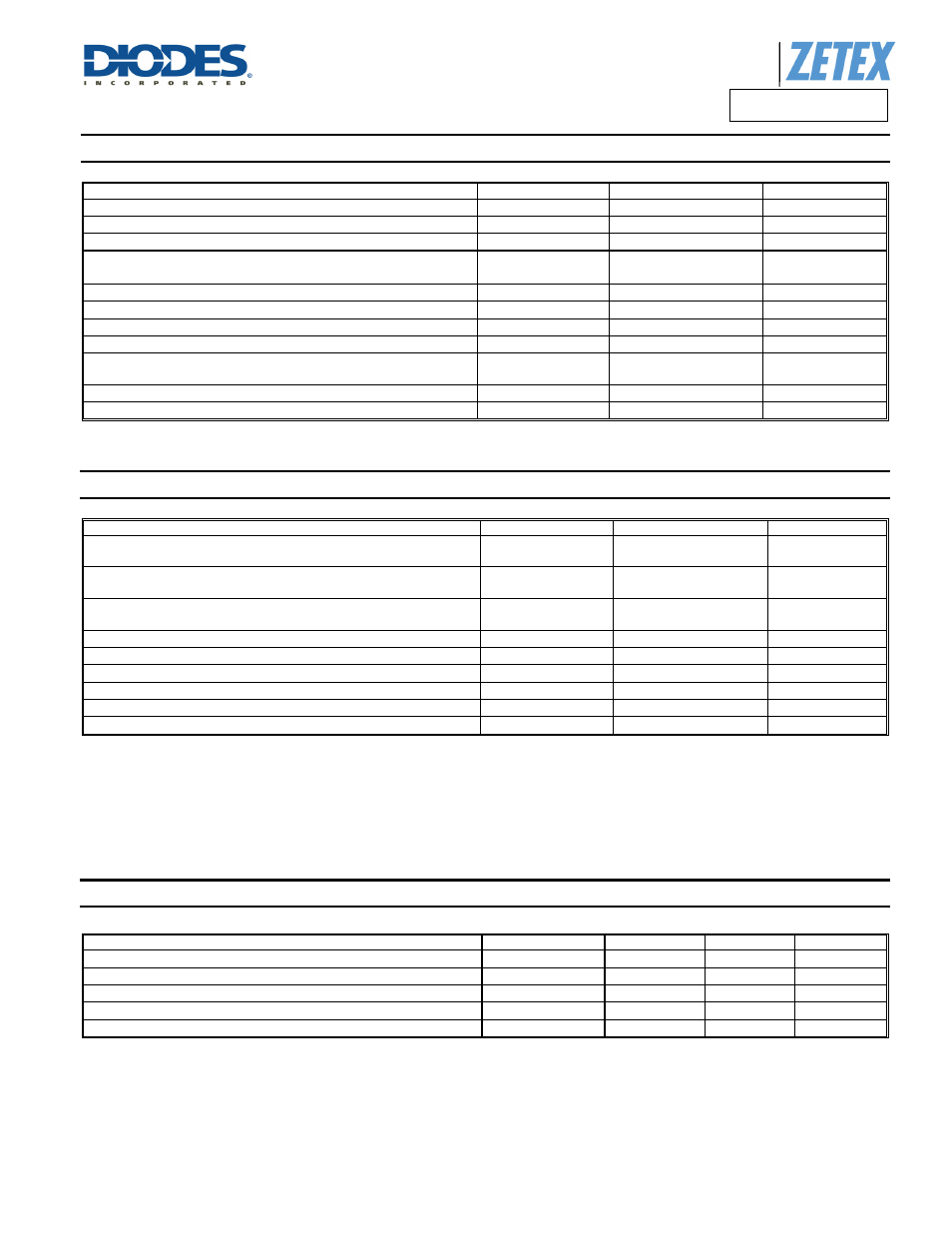
Maximum Ratings
(@T
A
= +25°C, unless otherwise specified.)
Characteristic Symbol
Value
Units
Continuous Drain-Source Voltage
V
DS
60 V
Drain-Source Voltage For Short Circuit Protection
V
DS(SC)
24 V
Continuous Input Voltage
V
IN
-0.5 ... +6
V
Continuous Input Current @ -0.2V ≤ V
IN
≤ 6V
Continuous Input Current @V
IN
< -0.2V or V
IN
> 6V
I
IN
No limit
│I
IN
│≤2
mA
Pulsed Drain Current @V
IN
= 3.3V ( Note 7)
I
DM
5 A
Pulsed Drain Current @V
IN
= 5V ( Note 7)
I
DM
6 A
Continuous Source Current (Body Diode) (Note 5)
I
S
2.5 A
Pulsed Source Current (Body Diode)
I
SM
10 A
Unclamped Single Pulse Inductive Energy,
T
J
= +25
C, I
D
= 0.5A, V
DD
= 24V
E
AS
210 mJ
Electrostatic Discharge (Human Body Model)
V
ESD
4000 V
Charged Device Model
V
CDM
1000 V
Thermal Characteristics
(@T
A
= +25°C, unless otherwise specified.)
Characteristic Symbol
Value
Units
Power Dissipation at T
A
= +25
C (Notes 5 & 8)
Linear Derating Factor
P
D
1.16
9.28
W
mW/
C
Power Dissipation at T
A
= +25
C (Notes 5 & 9)
Linear Derating Factor
P
D
1.67
13.3
W
mW/
C
Power Dissipation at T
A
= +25
C (Notes 6 & 8)
Linear Derating Factor
P
D
2.13
17
W
mW/
C
Thermal Resistance, Junction to Ambient (Notes 5 & 8)
R
θJA
108
C/W
Thermal Resistance, Junction to Ambient (Notes 5 & 9)
R
θJA
75
C/W
Thermal Resistance, Junction to Case (Notes 6 & 8)
R
θJC
58.7
C/W
Thermal Resistance, Junction to Case (Note 10)
R
θJC
26.5
C/W
Operating Temperature Range
T
J
-40 to +150
C
Storage Temperature Range
T
STG
-55 to +150
C
Notes:
5. For a dual device surface mounted on a 25mm x 25mm single sided 1oz weight copper split down the middle on 1.6mm FR4 board, in still air conditions.
6. For a dual device surface mounted on FR4 PCB measured at t≤ 10sec
7. Repetitive rating25mm x 25mm FR4 PCB, D = 0.02, Pulse width = 300µs – pulse width limited by junction temperature. Refer to transient thermal
impedance graph.
8. For a dual device with one active die.
9. For a dual device with 2 active die running at equal power.
10. Thermal resistance from junction to the mounting surface of the drain pin.
Recommended Operating Conditions
The ZXMS6005DT8 is optimized for use with µC operating from 3.3V and 5V supplies.
Characteristic Symbol
Min
Max
Unit
Input Voltage Range
V
IN
0 5.5 V
Ambient Temperature Range
T
A
-40 125 °C
High Level Input Voltage for MOSFET to be on
V
IH
3 5.5 V
Low Level Input Voltage for MOSFET to be off
V
IL
0 0.7 V
Peripheral Supply Voltage (voltage to which load is referred)
V
P
0 24 V