Electrical characteristics q2 p-channel – Diodes ZXMC10A816N8 User Manual
Page 7
ZXMC10A816N8
Document number: DS33497 Rev. 2 - 2
7 of 11
March 2013
© Diodes Incorporated
ZXMC10A816N8
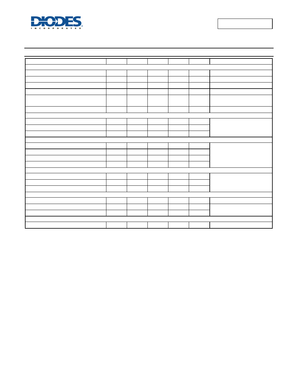
Electrical Characteristics Q2 P-Channel
(@T
A
= +25°C, unless otherwise specified.)
Parameter Symbol
Min
Typ
Max
Unit
Conditions
Static
Drain-Source Breakdown Voltage
V
(BR)DSS
-100 — — V
I
D
= -250µA, V
GS
= 0V
Zero Gate Voltage Drain current
I
DSS
— — -0.5 µA
V
DS
= -100V, V
GS
= 0V
Gate-Body Leakage
I
GSS
— — 100 nA
V
GS
=
20V, V
DS
= 0V
Gate-Source Threshold Voltage
V
GS(th)
-2.0 — -3.0 V
I
D
= -250µA, V
DS
= V
GS
Static Drain-Source On-State Resistance
(a)
R
DS(ON)
—
0.170
0.250
0.235
0.320
Ω
V
GS
= -10V, I
D
= -1.0A
V
GS
= -4.5V, I
D
= -0.5A
Forward Transconductance
(a) (c)
g
fs
— 4.7 — S
V
DS
= -15V, I
D
= -2.1A
Dynamic Capacitance
(c)
Input Capacitance
C
iss
— 717 — pF
V
DS
= -50V, V
GS
= 0V
f = 1MHz
Output Capacitance
C
oss
— 55 — pF
Reverse Transfer Capacitance
C
rss
— 46 — pF
Switching
(b) (c)
Turn-On-Delay Time
t
d(ON)
— 4.3 — ns
V
DD
= -50V, V
GS
= -10V
I
D
= -1A
R
G
6.0,
Rise Time
t
r
— 5.2 — ns
Turn-Off Delay Time
t
d(OFF)
— 20 — ns
Fall Time
t
f
— 12 — ns
Gate Charge
(c)
Total Gate Charge
Q
g
— 16.5 — nC
V
DS
= -50V, V
GS
= -10V
I
D
= -2.1A
Gate-Source Charge
Q
gs
— 2.5 — nC
Gate-Drain Charge
Q
gd
— 5.4 — nC
Source–Drain Diode
Diode Forward Voltage
(a)
V
SD
— -0.85
-0.95 V
I
S
= -1.7A, V
GS
= 0V
Reverse Recovery Time
(c)
t
rr
— 43 — ns
I
S
= -1.7A, di/dt
= 100A/
s
Reverse Recovery Charge
(c)
Q
rr
— 77 — nC
Gate Resistance
Gate Resistance
R
G
0 — 100
V
DS
= 0V, V
GS
= 0V, f = 1.0MHz
Notes:
(a) Measured under pulsed conditions. Pulse width
300
s; duty cycle
2%.
(b) Switching characteristics are independent of operating junction temperature.
(c) For design aid only, not subject to production testing.