Source-drain diode, Zxmc3a18dn8, P-channel electrical characteristics (at t – Diodes ZXMC3A18DN8 User Manual
Page 7: 25°c unless otherwise stated)
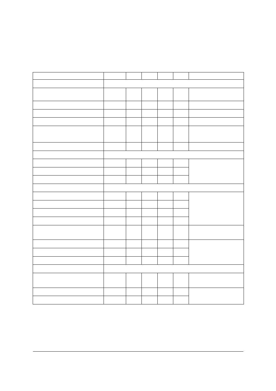
ZXMC3A18DN8
© Zetex Semiconductors plc 2007
P-channel
Electrical characteristics (at T
amb
= 25°C unless otherwise stated)
Parameter
Symbol
Min.
Typ.
Max.
Unit
Conditions
Static
Drain-source breakdown
voltage
V
(BR)DSS
-30
V
I
D
= -250
A, V
GS
=0V
Zero gate voltage drain current I
DSS
-1.0
A V
DS
= -30V, V
GS
=0V
Gate-body leakage
I
GSS
100
nA
V
GS
=±20V, V
DS
=0V
Gate-source threshold voltage
V
GS(th)
-1.0
V
I
D
= -250
A, V
DS
=V
GS
Static drain-source on-state
resistance
(*)
NOTES:
(*) Measured under pulsed conditions. Pulse width
Յ300s; duty cycle Յ2%.
R
DS(on)
0.035
W
V
GS
= -10V, I
D
= -4.8A
0.050
V
GS
= -4.5V, I
D
= -4.0A
Forward transconductance
g
fs
8.6
S
V
DS
= -15V, I
D
= -4.8A
Input capacitance
C
iss
1603
pF
V
DS
= -15V, V
GS
=0V
f=1MHz
Output capacitance
C
oss
434
pF
Reverse transfer capacitance
C
rss
388
pF
Switching
(†) (‡)
(†) Switching characteristics are independent of operating junction temperature.
(‡) For design aid only, not subject to production testing.
Turn-on-delay time
t
d(on)
4.8
ns
V
DD
= -15V, I
D
= -1A
R
G
@ 6.0
⍀, V
GS
= 10V
Rise time
t
r
9.5
ns
Turn-off delay time
t
d(off)
60
ns
Fall time
t
f
38
ns
Gate charge
Q
g
25
nC
V
DS
= -15V, V
GS
= -5V
I
D
= -4.8A
Total gate charge
Q
g
45
nC
V
DS
= -15V, V
GS
= -10V
I
D
= -4.8A
Gate-source charge
Q
gs
5.1
nC
Gate drain charge
Q
gd
11.5
nC
Source-drain diode
Diode forward voltage
V
SD
0.82
-0.95
V
T
j
=25°C, I
S
= -3.7
V
GS
=0V
Reverse recovery time
t
rr
32.5
ns
T
j
=25°C, I
S
= -2.2,
di/dt=100A/
s
Reverse recovery charge
Q
rr
18.4
nC