Zxmn6a25n8 – Diodes ZXMN6A25N8 User Manual
Page 4
ZXMN6A25N8
Issue 1 - April 2008 4
© Zetex Semiconductors plc 2008
www.zetex.com
Electrical characteristics (at T
amb
= 25°C unless otherwise stated)
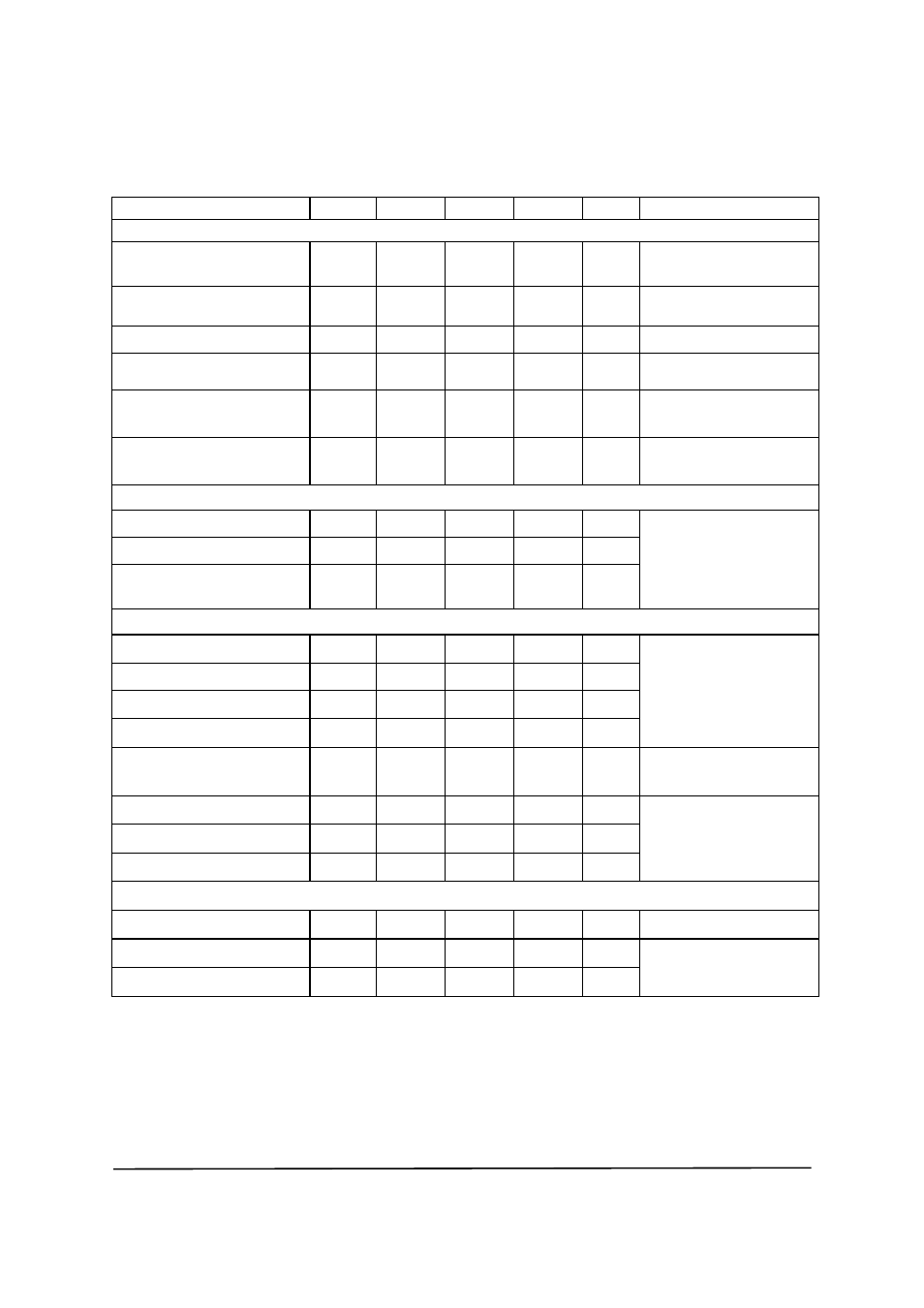
Parameter Symbol
Min.
Typ.
Max.
Unit
Conditions
Static
Drain-Source breakdown
voltage
V
(BR)DSS
60 V
I
D
=250
μA, V
GS
=0V
Zero gate voltage drain
current
I
DSS
1.0
µA
V
DS
=60V, V
GS
=0V
Gate-Body leakage
I
GSS
100
nA
V
GS
=
±
20V, V
DS
=0V
Gate-Source threshold
voltage
V
GS(th)
1 3
V
I
D
=250
μA, V
DS
=V
GS
Static Drain-Source
on-state resistance
(
*
)
R
DS(on)
0.050
0.070
Ω
V
GS
= 10V, I
D
= 3.6A
V
GS
= 4.5V, I
D
= 3.0A
Forward
Transconductance
(
*
) (†)
g
fs
10.2
S
V
DS
= 15V, I
D
= 4.5A
Dynamic
(†)
Input capacitance
C
iss
1063
pF
Output capacitance
C
oss
104
pF
Reverse transfer
capacitance
C
rss
64
pF
V
DS
= 30V, V
GS
=0V
f=1MHz
Switching
(‡) (†)
Turn-on-delay time
t
d(on)
3.8
ns
Rise time
t
r
4.0
ns
Turn-off delay time
t
d(off)
26.2
ns
Fall time
t
f
10.6
ns
V
DD
= 30V, V
GS
= 10V
I
D
= 1A
R
G
≅ 6.0Ω,
Gate charge
Q
g
11.0
nC
V
DS
= 30V, V
GS
= 5V
I
D
= 4.5A
Total gate charge
Q
g
20.4
nC
Gate-Source charge
Q
gs
4.1
nC
Gate-Drain charge
Q
gd
5.1
nC
V
DS
= 30V, V
GS
= 10V
I
D
= 4.5A
Source–Drain diode
Diode forward voltage
(
*
)
V
SD
0.85 0.95 V
I
S
= 5.5A,V
GS
=0V
Reverse recovery time
(‡)
t
rr
22.0
ns
Reverse recovery charge
(‡)
Q
rr
21.4
nC
I
S
= 2.2A,di/dt=100A/
μs
NOTES:
(*) Measured under pulsed conditions. Pulse width
≤ 300μs; duty cycle ≤ 2%.
(†)Switching characteristics are independent of operating junction temperature.
(‡)For design aid only, not subject to production testing