Zxmn6a25n8 – Diodes ZXMN6A25N8 User Manual
Page 2
ZXMN6A25N8
Issue 1 - April 2008 2
© Zetex Semiconductors plc 2008
www.zetex.com
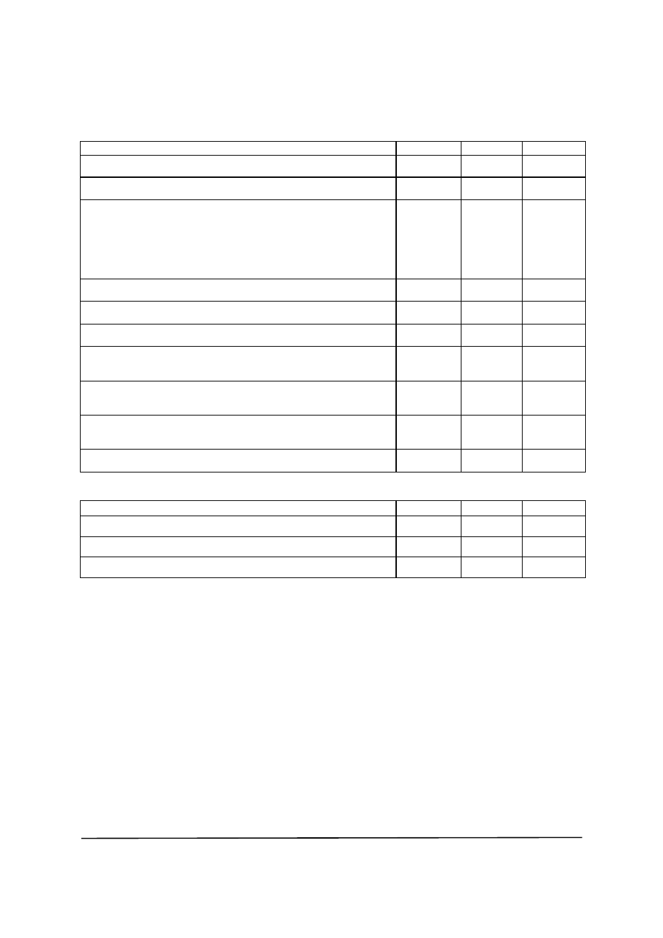
Absolute maximum ratings
Parameter Symbol
Limit
Unit
Drain-Source voltage
V
DSS
60
V
Gate-Source voltage
V
GS
± 20
V
Continuous Drain current @ V
GS
= 10V; T
A
=25
°C
(b)
@ V
GS
= 10V; T
A
=70
°C
(b)
@ V
GS
= 10V; T
A
=25
°C
(a)
@ V
GS
= 10V; T
L
=25
°C
(a)(d)
I
D
5.7
4.5
4.3
7.0
A
Pulsed Drain current
(c)
I
DM
25.7 A
Continuous Source current (Body diode)
(b)
I
S
4.1 A
Pulsed Source current (Body diode)
(c)
I
SM
25.7 A
Power dissipation at T
A
=25
°C
(a)
Linear derating factor
P
D
1.56
12.5
W
mW/
°C
Power dissipation at T
A
=25
°C
(b)
Linear derating factor
P
D
2.8
22.2
W
mW/
°C
Power dissipation at T
L
=25
°C
(d)
Linear derating factor
P
D
4.14
33.1
W
mW/
°C
Operating and storage temperature range
T
j
, T
stg
-55 to 150
°C
Thermal resistance
Parameter Symbol
Value
Unit
Junction to ambient
(a)
R
θJA
80
°C/W
Junction to ambient
(b)
R
θJA
45
°C/W
Junction to lead
(d)
R
θJL
30.2
°C/W
NOTES:
(a) For a device surface mounted on 25mm x 25mm x 1.6mm FR4 PCB with high coverage of single sided 1oz copper, in still
air conditions.
(b) Mounted on FR4 PCB measured at t
≤ 10 sec.
(c) Repetitive rating on 25mm x 25mm FR4 PCB, D=0.02, pulse width 300us – pulse width limited by maximum junction
temperature.
(d) Thermal resistance from junction to solder-point (at the end of the drain lead).