Descriptions of the normal operation – Diodes ZXGD3103N8 User Manual
Page 8
ZXGD3103N8
ZXGD3103N8
Document number: DS32255 Rev. 2 - 2
8 of 12
November 2011
© Diodes Incorporated
A Product Line of
Diodes Incorporated
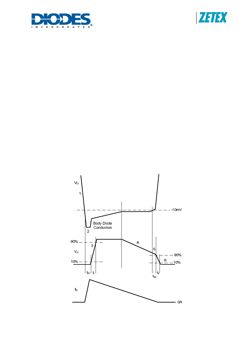
Descriptions of the normal operation
The operation of the device is described step-by-step with reference to the timing diagram in Figure 3.
1. The detector monitors the MOSFET Drain-Source voltage.
2. When, due to transformer action, the MOSFET body diode is forced to conduct there is approximately -
0.8V on the Drain pin.
3. The detector outputs a positive voltage with respect to ground, this voltage is then fed to the MOSFET
driver stage and current is sourced out of the GATE pin.
4. The controller goes into proportional gate drive control — the GATE output voltage is proportional to the
on-resistance-induced Drain-Source voltage drop across the MOSFET. Proportional gate drive ensures that
MOSFET conducts for majority of the conduction cycle and minimizes body diode conduction time.
5. As the Drain current decays linearly toward zero, proportional gate drive control reduces the Gate voltage
so the MOSFET can be turned off rapidly at zero current crossing. The GATE voltage is removed when the
Drain-Source voltage crosses the detection threshold voltage to minimize reverse current flow.
6. At zero Drain current, the controller GATE output voltage is pulled low to V
G(off)
to ensure that the
MOSFET is off.
Figure 4 shows typical operating waveforms for ZXGD3103 driving a MOSFET with Q
g(TOT)
= 82nC in a
Flyback converter operating in critical conduction mode.
Figure 3. Timing diagram for a critical conduction mode Flyback converter