Electrical characteristics at, 25°c; v, 10v; r – Diodes ZXGD3103N8 User Manual
Page 3: 3k ω; r, 3k ω, Switching performance (“) for q, Tot) = 82nc
ZXGD3103N8
ZXGD3103N8
Document number: DS32255 Rev. 2 - 2
3 of 12
November 2011
© Diodes Incorporated
A Product Line of
Diodes Incorporated
Electrical characteristics at
T
A
= 25°C; V
CC
= 10V; R
BIAS
= 3.3k
Ω; R
REF
= 4.3k
Ω
Parameter Symbol
Conditions
Min.
Typ.
Max.
Unit
Input and supply characteristics
Operating current
I
OP
V
D
≤ -200m V
-
2.16
-
mA
V
D
≥ 0V
-
5.16
-
Gate Driver
Turn-off Threshold
Voltage(**)
V
T
V
G
= 1V, (*)
-16 -10 0 mV
GATE output voltage (**)
V
G(off)
V
D
≥ 0V, (*)
- 0.73 1
V
V
G
V
D
= -50mV, (
g)
6.0 7.2 -
V
D
= -100mV, (
g)
8.8 9.2 -
V
D
≤ -150mV, (g)
9.2 9.4 -
V
D
≤ -200mV, (g)
9.3 9.5 -
Switching performance (“) for Q
G
(tot) = 82nC
Turn on Propagation delay
t
d1
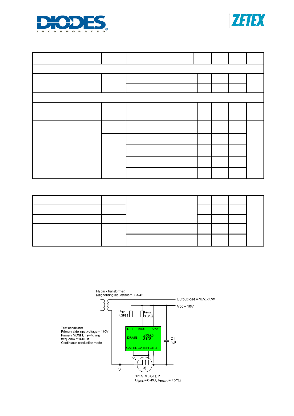
Refer to switching waveforms
in Fig. 3
150
ns
Turn off Propagation delay
t
d2
15
Gate rise time
t
r
450
Gate fall time
t
f
Continuous Conduction Mode
21
Discontinuous Conduction
Mode
17
Notes:
(**)
GATEH connected to GATEL
(*)
R
H
= 100k
Ω, R
L
= O/C
(
g) R
L
= 100k
Ω, R
H
= O/C
(“) refer to test circuit below