Schematic symbol and pin out details – Diodes ZXGD3103N8 User Manual
Page 4
ZXGD3103N8
ZXGD3103N8
Document number: DS32255 Rev. 2 - 2
4 of 12
November 2011
© Diodes Incorporated
A Product Line of
Diodes Incorporated
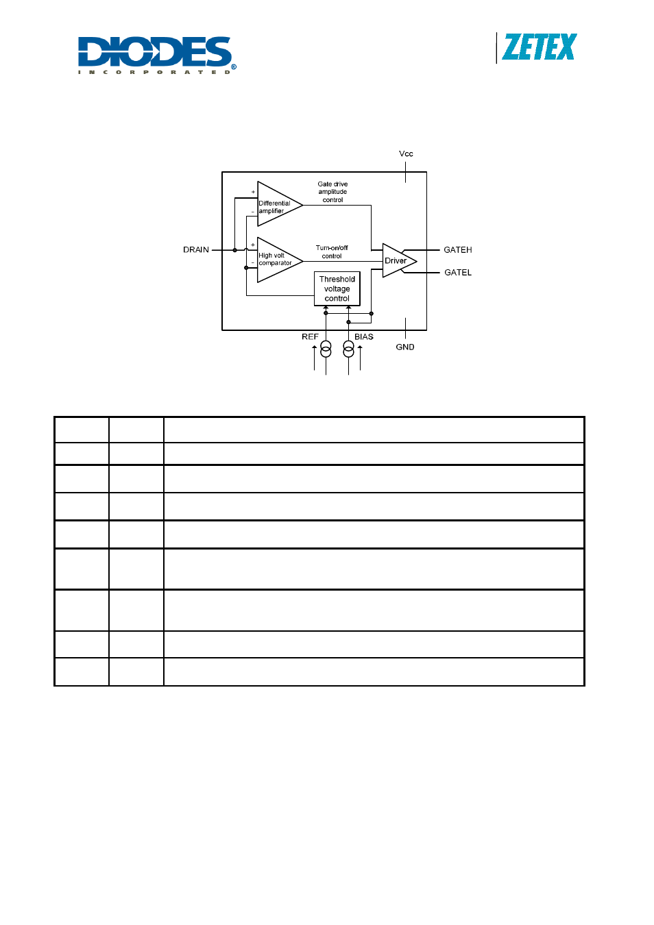
Schematic Symbol and Pin Out Details
Pin No.
Name
Description and function
1
NC
No Internal connection
2
REF
Reference
This pin is connected to V
CC
via resistor, R
REF
3 GATEL
Gate turn off
This pin sinks current, I
SINK
, from the synchronous MOSFET Gate.
4
GATEH
Gate turn on
This pin sources current, I
SOURCE
, to the synchronous MOSFET Gate.
5 V
CC
Power Supply
This is the supply pin. It is recommended to decouple this point to ground closely
with a ceramic capacitor.
6 GND
Ground
This is the ground reference point. Connect to the synchronous MOSFET Source
terminal.
7 BIAS
Bias
This pin is connected to V
CC
via resistor, R
BIAS
.
8
DRAIN
Drain connection
This pin connects directly to the synchronous MOSFET Drain terminal.
- PDS3200 (5 pages)
- PDS340 (5 pages)
- PDS340Q (5 pages)
- PDS360 (5 pages)
- PDS360Q (5 pages)
- PDS4150 (4 pages)
- PDS3100Q (5 pages)
- PDS3100 (5 pages)
- PDS1240CTL (5 pages)
- PDS1045 (5 pages)
- PDS1040L (5 pages)
- PDS1040CTL (5 pages)
- PDS1040 (5 pages)
- PD3S230L (5 pages)
- PD3S230H (3 pages)
- PDS5100Q (5 pages)
- PDS835L (5 pages)
- PDS760 (5 pages)
- PDS560 (5 pages)
- PDS540 (5 pages)
- PDS5100H (5 pages)
- PDS5100 (5 pages)
- PDS4200H (6 pages)
- SBL3060CTP (4 pages)
- SBL30L30CT (3 pages)
- SBL3045CTP (4 pages)
- SBL3040CTP (4 pages)
- SBL2060CTP (4 pages)
- SBL2030CT - SBL2060CT (3 pages)
- SBL2045CTP (4 pages)
- SBL1060CTP (4 pages)
- SBL1040CTP (4 pages)
- SBG3030CT - SBG3045CT (5 pages)
- SB520 - SB560 (3 pages)
- SB370 - SB3100 (3 pages)
- SB320 - SB360 (3 pages)
- SBR10U100CT (5 pages)
- SBR10U150CT (5 pages)
- SBR10A45SP5 (5 pages)
- SBR1060CT (5 pages)
- SBR1045SP5 (5 pages)
- SBR1045SD1 (4 pages)
- SBR1045D1 (5 pages)
- SBR1045CTL (4 pages)
- SBR1040CT (5 pages)