Schematic symbol and pin out details – Diodes ZXGD3101N8 User Manual
Page 4
ZXGD3101N8
Document Number DS31945 Rev. 1 - 2
4 of 14
June 2010
© Diodes Incorporated
ZXGD3101N8
A Product Line of
Diodes Incorporated
S Y N C H R O N O U S R E C T I F I E R C O N T R O L L E R
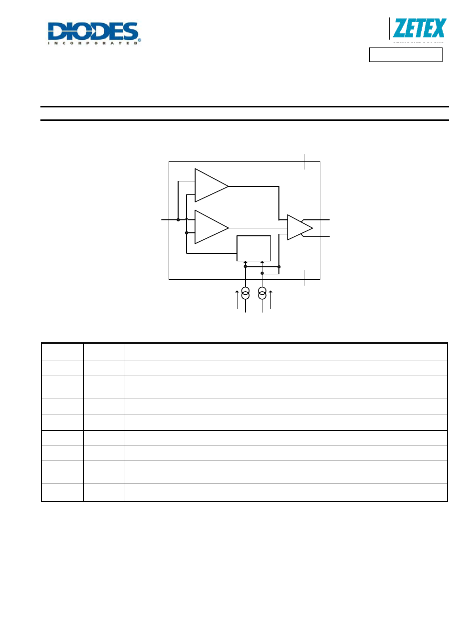
Schematic Symbol and Pin Out Details
Differential
amplifier
High volt
comparator
Threshold
voltage
control
Driver
Gate drive
amplitude
control
Turn-on/off
control
+
+
-
-
GATEH
GATEL
Vcc
GND
DRAIN
REF
BIAS
Pin No.
Symbol
Description and function
1
NC
No connection
This pin can be connected to GND
2
REF
Reference
This pin is connected to V
CC
via resistor, R
REF
. R
REF
should be selected to source approximately 3mA into this pin.
(Note 8)
3
GATEL
Gate turn off
This pin sinks current, I
SINK
, from the synchronous MOSFET Gate.
4
GATEH
Gate turn on
This pin sources current, I
SOURCE
, to the synchronous MOSFET Gate.
5
V
CC
Power Supply
This is the supply pin. It is recommended to decouple this point to ground closely with a ceramic capacitor.
6
GND
Ground
This is the ground reference point. Connect to the synchronous MOSFET Source terminal.
7
BIAS
Bias
This pin is connected to V
CC
via resistor, R
BIAS
. R
BIAS
should be selected to source 1.6 times I
REF
into this pin.
(Note 9)
8
DRAIN
Drain connection
This pin connects directly to the synchronous MOSFET Drain terminal.
Notes:
8. REF pin should be assumed to be at GND +0.7V.
9. BIAS pin should be assumed to be at GND +0.3V.