Electrical characteristics – Diodes ZXGD3101N8 User Manual
Page 3
ZXGD3101N8
Document Number DS31945 Rev. 1 - 2
3 of 14
June 2010
© Diodes Incorporated
ZXGD3101N8
A Product Line of
Diodes Incorporated
S Y N C H R O N O U S R E C T I F I E R C O N T R O L L E R
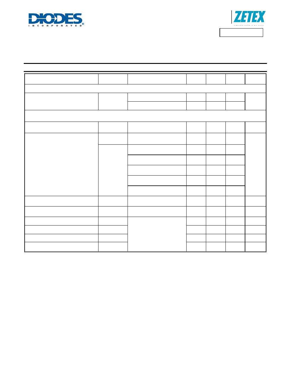
Electrical Characteristics
@T
A
= 25°C, V
CC
= 10V,
R
BIAS
=1.8k
Ω, R
REF
=3k
Ω
Parameter Symbol
Conditions
Min.
Typ.
Max.
Unit
Input and supply characteristics
Operating current
I
OP
V
DRAIN
≤ -200m V
- 3 -
mA
V
DRAIN
≥ 0V
- 8 -
Gate Driver
Turn-off Threshold Voltage(Note 4)
V
T
V
G
= 1V, (Note 5)
-45 -16 0 mV
GATE output voltage (Note 4)
V
G(off)
V
DRAIN
≥ 0V, (Note 5)
- 0.6 1
V
V
G
V
DRAIN
= -60mV, (Note 6)
5.0 7.5 -
V
DRAIN
= -80mV, (Note 6)
7.0 8.5 -
V
DRAIN
= -100mV, (Note 6)
8.4 9 -
V
DRAIN
≤ -140mV, (Note 6)
9.2 9.4 -
V
DRAIN
≤ -200mV, (Note 6)
9.3 9.5 -
GATEH peak source current
I
SOURCE
V
GH
= 1V
2.5 - A
GATEL peak sink current
I
SINK
V
GL
= 5V
2.5 - A
Turn on Propagation delay
t
d1
C
L
= 2.2nF, (Notes 6 and 7)
525
ns
Turn off Propagation delay
t
d2
15
ns
Gate rise time
t
r
305
ns
Gate fall time
t
f
20
ns
Notes:
4. GATEH connected to GATEL
5. R
H
= 100k
Ω, R
L
= O/C
6. R
L
= 100k
Ω, R
H
= O/C
7. Refer to Fig 6: test circuit and Fig 7: timing diagram on Page 12