Maximum ratings, Thermal characteristics, Esd rating – Diodes ZXGD3101N8 User Manual
Page 2
ZXGD3101N8
Document Number DS31945 Rev. 1 - 2
2 of 14
June 2010
© Diodes Incorporated
ZXGD3101N8
A Product Line of
Diodes Incorporated
S Y N C H R O N O U S R E C T I F I E R C O N T R O L L E R
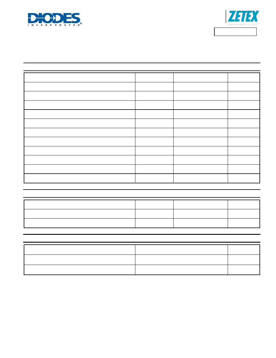
Maximum Ratings
Parameter Symbol
Limit
Unit
Supply voltage
(Note 1)
V
CC
15 V
Continuous Drain pin voltage (Note 1)
V
D
-3 to180
V
GATEH and GATEL output Voltage (Note 1)
V
G
-3 to V
CC
+ 3
V
Driver peak source current
I
SOURCE
4 A
Driver peak sink current
I
SINK
7 A
Reference current
I
REF
25 mA
Bias voltage
V
BIAS
V
CC
V
Bias current
I
BIAS
100 mA
Power dissipation at T
A
=25
°C
P
D
490 mW
Operating junction temperature
T
J
-40 to +150
°C
Storage temperature
T
STG
-50 to +150
°C
Thermal Characteristics
Parameter Symbol
Value
Unit
Junction to ambient (Note 2)
R
θJA
255 °C/W
Junction to lead (Note 3)
R
θlA
120 °C/W
ESD Rating
Model Rating
Unit
Human Body
4000 V
Machine
400 V
Notes:
1.All voltages are relative to GND pin
2. Mounted on minimum 1oz weight copper on FR4 PCB in still air conditions.
3. Output Drivers - Junction to solder point at end of the lead 5 and 6