Diodes ZXTD6717E6 User Manual
Page 2
ISSUE 2 - JULY 2001
ZXTD6717E6
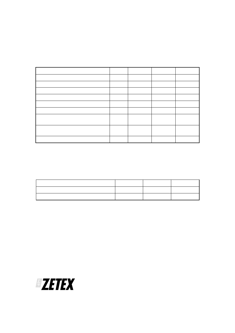
THERMAL RESISTANCE
PARAMETER
SYMBOL
VALUE
UNIT
Junction to Ambient (a)
R
θ
JA
125
°C/W
Junction to Ambient (b)
R
θ
JA
45
°C/W
NOTES
(a) For a device surface mounted on 25mm x 25mm FR4 PCB with high coverage of single sided 1oz copper,
in still air conditions
(b) For a device surface mounted on FR4 PCB measured at t
р5 secs.
2
ABSOLUTE MAXIMUM RATINGS.
PARAMETER
SYMBOL
LIMIT NPN
LIMIT PNP
UNIT
Collector-Base Voltage
V
CBO
15
-12
V
Collector-Emitter Voltage
V
CEO
15
-12
V
Emitter-Base Voltage
V
EBO
5
-5
V
Peak Pulse Current
I
CM
5
-3
A
Continuous Collector Current
I
C
1.5
-1.25
A
Base Current
I
B
200
-200
mA
Power Dissipation at TA=25°C (a)
Linear Derating Factor
P
D
1.1
8.8
1.1
8.8
W
mW/°C
Power Dissipation at TA=25°C (b)
Linear Derating Factor
P
D
1.7
13.6
1.7
13.6
W
mW/°C
Operating and Storage Temperature Range
T
j
:T
stg
-55 to +150
-55 to +150
°C
- PDS3200 (5 pages)
- PDS340 (5 pages)
- PDS340Q (5 pages)
- PDS360 (5 pages)
- PDS360Q (5 pages)
- PDS4150 (4 pages)
- PDS3100Q (5 pages)
- PDS3100 (5 pages)
- PDS1240CTL (5 pages)
- PDS1045 (5 pages)
- PDS1040L (5 pages)
- PDS1040CTL (5 pages)
- PDS1040 (5 pages)
- PD3S230L (5 pages)
- PD3S230H (3 pages)
- PDS5100Q (5 pages)
- PDS835L (5 pages)
- PDS760 (5 pages)
- PDS560 (5 pages)
- PDS540 (5 pages)
- PDS5100H (5 pages)
- PDS5100 (5 pages)
- PDS4200H (6 pages)
- SBL3060CTP (4 pages)
- SBL30L30CT (3 pages)
- SBL3045CTP (4 pages)
- SBL3040CTP (4 pages)
- SBL2060CTP (4 pages)
- SBL2030CT - SBL2060CT (3 pages)
- SBL2045CTP (4 pages)
- SBL1060CTP (4 pages)
- SBL1040CTP (4 pages)
- SBG3030CT - SBG3045CT (5 pages)
- SB520 - SB560 (3 pages)
- SB370 - SB3100 (3 pages)
- SB320 - SB360 (3 pages)
- SBR10U100CT (5 pages)
- SBR10U150CT (5 pages)
- SBR10A45SP5 (5 pages)
- SBR1060CT (5 pages)
- SBR1045SP5 (5 pages)
- SBR1045SD1 (4 pages)
- SBR1045D1 (5 pages)
- SBR1045CTL (4 pages)
- SBR1040CT (5 pages)