Thermal characteristics and derating information, Safe operating area, Derating curve – Diodes ZXTC2062E6 User Manual
Page 3: Safe operating area pulse power dissipation, Transient thermal impedance
ZXTC2062E6
Document Number: DS33647 Rev: 2 - 2
3 of 9
February 2013
© Diodes Incorporated
ZXTC2062E6
ADVAN
CE I
N
F
O
RM
ATI
O
N
A Product Line of
Diodes Incorporated
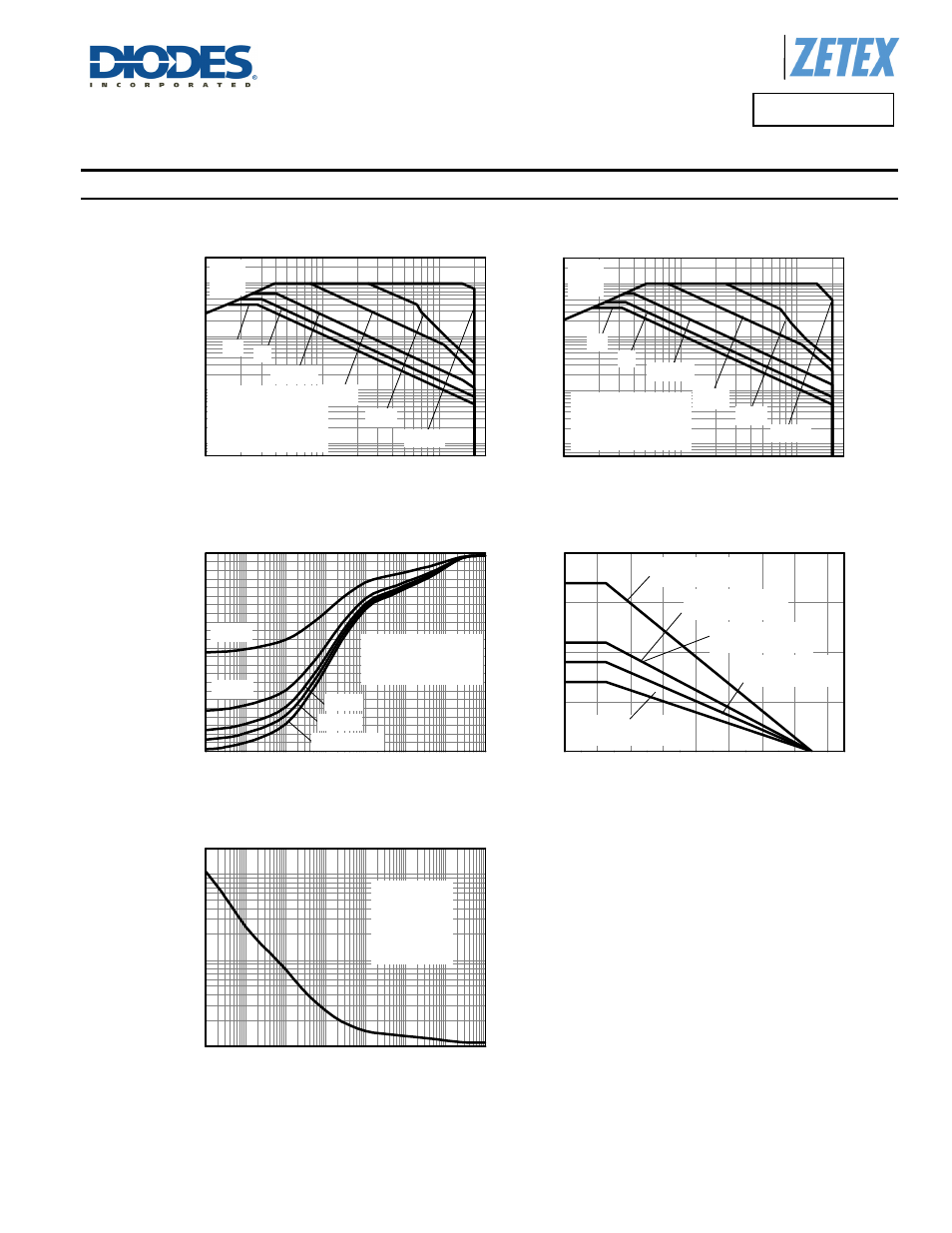
Thermal Characteristics and Derating Information
100µ
1m
10m 100m
1
10
100
1k
0
10
20
30
40
50
60
70
80
90
100
110
0.1
1
10
10m
100m
1
10
100m
1
10
10m
100m
1
10
NPN
Tamb=25°C
50mm x 50mm 2oz FR4
One active die
R
DS(on)
Limit
100µs
1ms
10ms
100ms
1s
DC
Safe Operating Area
I
C
Co
llec
tor
Curr
ent
(A
)
V
CE
Collector-Emitter Voltage (V)
0
20
40
60
80 100 120 140 160
0.0
0.5
1.0
1.5
2.0
15mm x 15mm 1oz FR4
One activ die
25mm x 25mm 1oz FR4
One activ die
50mm x 50mm 2oz FR4
One activ die
25mm x 25mm 1oz FR4
two activ die
50mm x 50mm 2oz FR4
One activ die, t < 5 sec
Derating Curve
Temperature (°C)
M
ax P
owe
r Di
ssi
pa
tio
n (W)
100µ
1m
10m 100m
1
10
100
1k
1
10
100
Single Pulse
Tamb=25°C
50mm x 50mm
2oz FR4
One active die
Safe Operating Area
Pulse Power Dissipation
Pulse Width (s)
M
a
x P
ower Di
ss
ip
at
ion (W)
Tamb=25°C
50mm x 50mm 2oz FR4
One activ die
D=0.1
D=0.05
Single Pulse
D=0.2
D=0.5
Transient Thermal Impedance
Pulse Width (s)
T
hermal Res
is
tan
ce
(°
C/
W)
PNP
Tamb=25°C
50mm x 50mm 2oz FR4
One active die
100µs
1ms
10ms
100ms
1s
DC
R
DS(on)
Limit
-V
CE
Collector-Emitter Voltage (V)
-I
C
Col
le
ct
or Current
(A
)